

High speed dynamic frequency divider
- Summary
- Abstract
- Description
- Claims
- Application Information
AI Technical Summary
Benefits of technology
Problems solved by technology
Method used
Image

Examples
Embodiment Construction
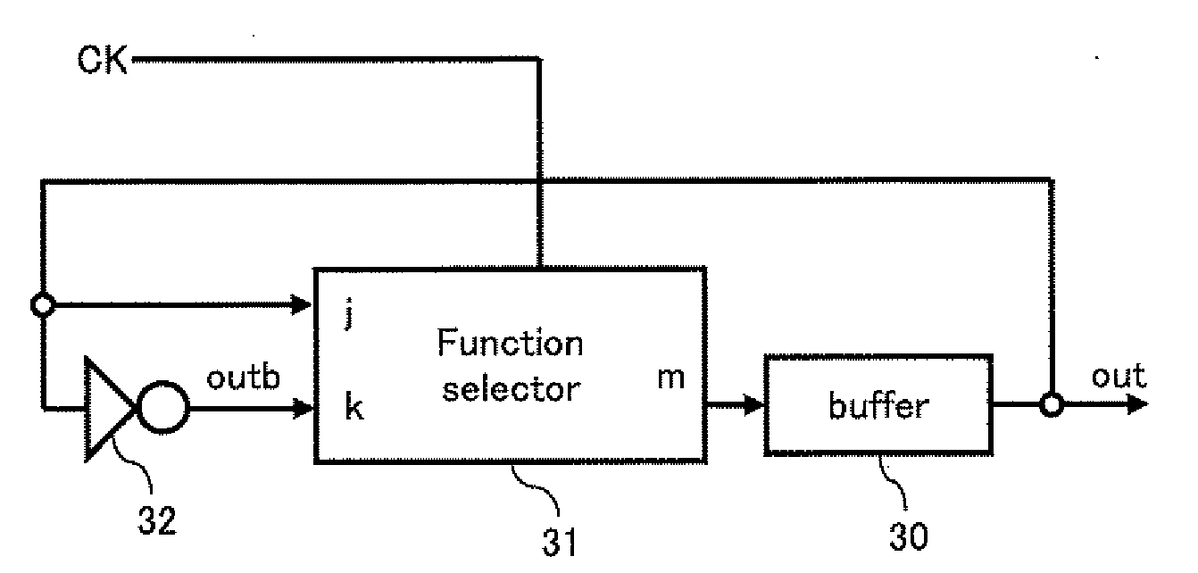
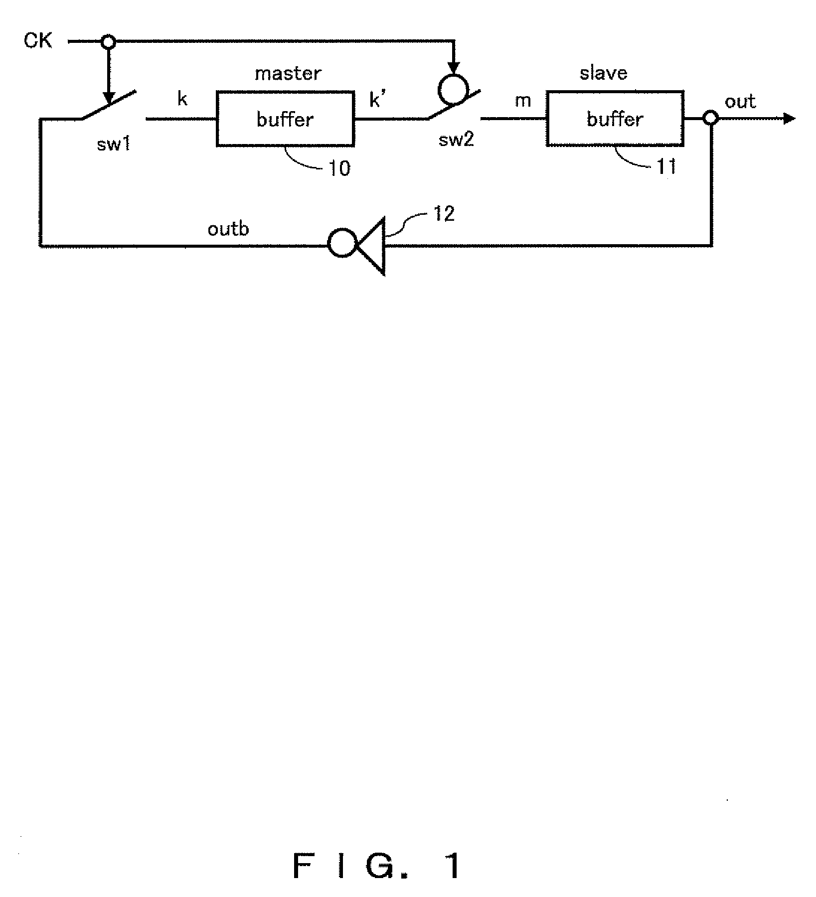
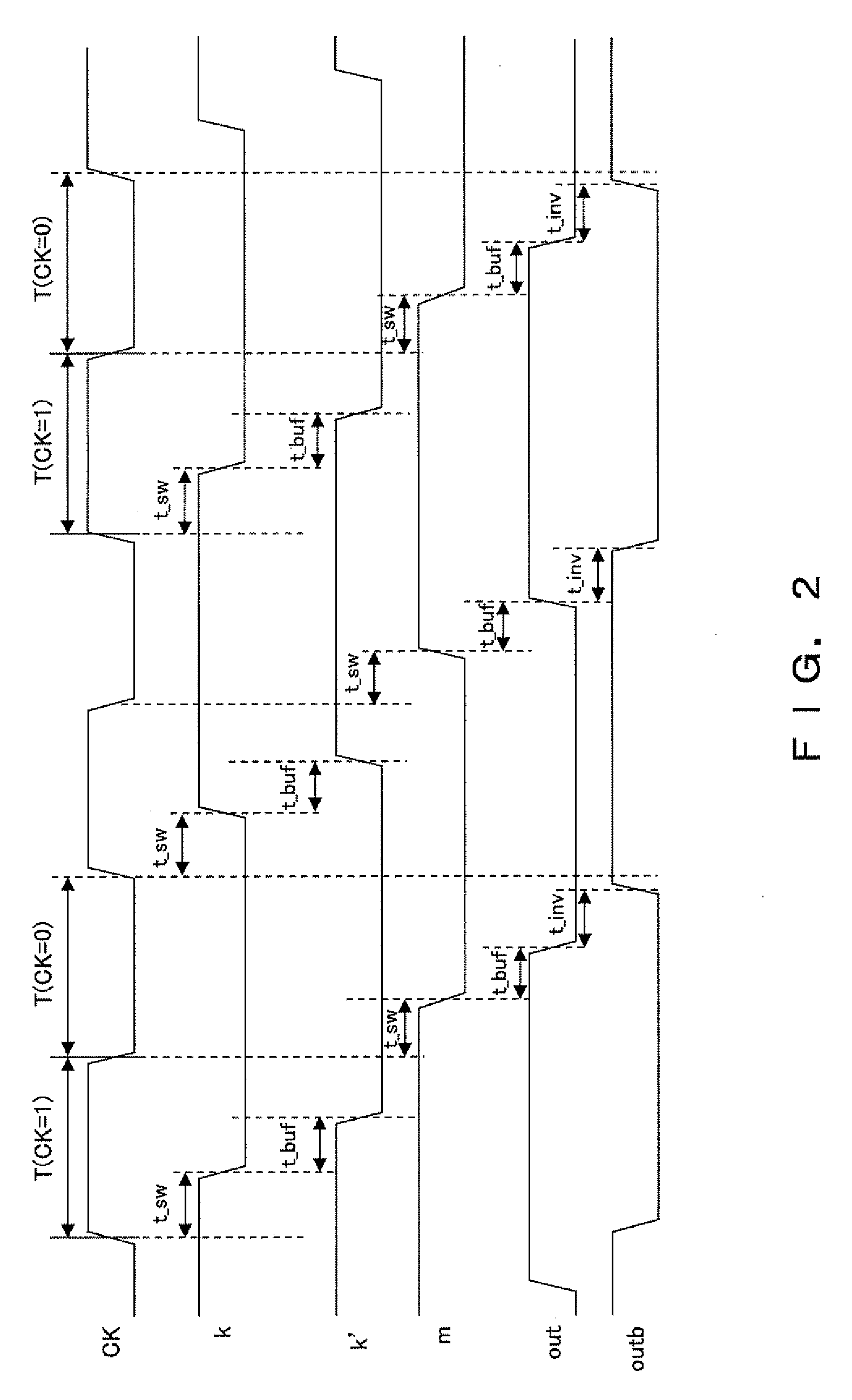
[0048]The FD of the present invention may be embedded in integrated circuits or be built with discrete elements. The FD of the present invention is also applicable to Clock Data Recovery (CDR) systems, logic systems (like ripple counters or ring counters), and / or transceivers, in which periodic clocks and / or signals are used to synchronize (retime) input data or internal data. In the frequency divider of the present invention, when the input clock signal (CK) is of logical “high”, one of the switches will close and the circuit will perform as a ring oscillator (oscillates once or flips). After a certain time period, the output value will begin to toggle and then completely change to a value that is the negation of the previous “output” value. When the input clock signal (CK) is of logical “low”, the corresponding switch will be turned off such that the updated output value can be held. However, since the CK signal should change to turn off the switch before the circuit oscillates mo...
PUM
 Abstract
Description
Claims
Application Information