Semiconductor device

a technology of semiconductor devices and resist masks, applied in semiconductor devices, diodes, electrical apparatus, etc., can solve the problems of lithography masks and resist masks used for actual implantation, the conversion difference between lithography masks and resist masks, and the breakdown voltage of devices, etc., to achieve the effect of low dopant concentration

Inactive Publication Date: 2007-11-29
KK TOSHIBA
View PDF9 Cites 150 Cited by
  • Summary
  • Abstract
  • Description
  • Claims
  • Application Information

AI Technical Summary

Benefits of technology

[0012] According to an aspect of the invention, there is provided a semiconductor device including: a semiconductor layer of a first conductivity type; a first semiconductor pillar region of the first conductivity type provided on a major surface of the semiconductor layer; a second semiconductor pillar region of a second conductivity type provided adjacent to the first semiconductor pillar region on the major surface of the semiconductor layer, the second semiconductor pillar region forming a periodic arrangement structure substantially parallel to the major surface of the semiconductor layer together with the first semiconductor pillar region; a first main electrode provided on a side opposite to the major surface of the semiconductor layer; a first semiconductor region of the second conductivity type selectively provided on the first semiconductor pillar region and the second semiconductor pillar region; a second semiconductor region of the first conductivity type selectively provided in a surface of the first semiconductor region; a second main electrode provided in contact with the first semiconductor region and the second semiconductor region; a control electrode provided on the first semiconductor region, the second semiconductor region, and the first semiconductor pillar region via an insulating film; and a high-resistance semiconductor layer provided on the semiconductor layer in an edge termination section surrounding the first semiconductor pillar region and the second semiconductor pillar region, the high-resistance semiconductor layer having a lower dopant concentration than the first semiconductor pillar region, a boundary region being provided between a device central region and the edge termination section, and the first semiconductor pillar region and the second semiconductor pillar region adjacent to the high-resistance semiconductor layer in the boundary region having a depth decreasing stepwise toward the edge termination section.
[0013] According to another aspect of the invention, there is provided a semiconductor device including: a first semiconductor layer of a first conductivity type; a first semiconductor pillar region of the first conductivity type provided on a major surface of the first semiconductor layer; a second semiconductor pillar region of a second conductivity type provided adjacent to the first semiconductor pillar region on the major surface of the first semiconductor layer, the second semiconductor pillar region forming a periodic arrangement structure substantially parallel to the major surface of the first semiconductor layer together with the first semiconductor pillar region; a first main electrode provided on a side opposite to the major surface of the first semiconductor layer; a first semiconductor region of the second conductivity type selectively provided on the first semiconductor pillar region and the second semiconductor pillar region; a second semiconductor region of the first conductivity type selectively provided in a surface of the first semiconductor region; a second main electrode provided in contact with the first semiconductor region and the second semiconductor region; a control electrode provided on the first semiconductor region, the second semiconductor region, and the first semiconductor pillar region via an insulating film; a second semiconductor layer of the first conductivity type provided on the first semiconductor layer in an edge termination section outside a device section including the periodic arrangement structure of the first semiconductor pillar region and the second semiconductor pillar region, the second semiconductor layer having a lower dopant concentration than the first semiconductor pillar region; and a buried guard ring layer of the second conductivity type semiconductor selectively buried in the second semiconductor layer.
[0014] According to another aspect of the invention, there is provided a semiconductor device including: a first semiconductor layer; a second semiconductor layer of a first conductivity type provided on a major surface side of the first semiconductor layer; a first main electrode provided on a side opposite to the major surface of the first semiconductor layer; a semiconductor region of a second conductivity type selectively provided in a surface of the second semiconductor layer; a second main electrode provided in contact with the semiconductor region; and a buried guard ring layer of the second conductivity type semiconductor selectively buried in the second semiconductor layer in an edge termination section outside the semiconductor region, the buried guard ring layer being depleted upon application of high voltage.

Problems solved by technology

Thus there is a tradeoff between the device breakdown voltage and the ON resistance.
However, in this structure, the superjunction structure is discontinuous between the device section and the edge termination section.
However, a conversion difference occurs between the lithography mask and the resist mask used for actual implantation.
Thus, unfortunately, the edge termination structure promising for high breakdown voltage in principle is difficult to realize and susceptible to process dispersion.
In this case, hot carriers generated by the high electric field degrades the field insulating film, and is likely to cause reliability degradation such as leak current variation, breakdown voltage variation, and breakdown.
Furthermore, if an avalanche breakdown occurs in the edge termination section during application of high voltage, carriers due to the avalanche current further increases the electric field peak, and unfortunately, is likely to cause current concentration and device breakdown.
Hence it is difficult to achieve high avalanche withstanding capability.
Hence, with a high electric field peak, a local avalanche breakdown occurs, and is likely to cause device breakdown.
Thus it is difficult to achieve high recovery capability.

Method used


Image

  • Semiconductor device
  • Semiconductor device
  • Semiconductor device

Examples


first embodiment

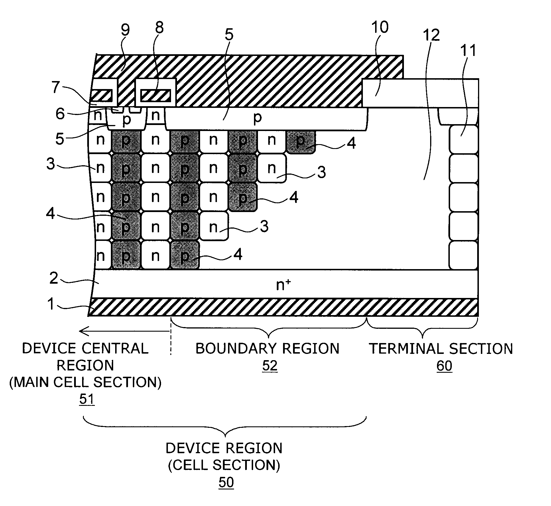
[0070]FIG. 1 is a schematic view illustrating the cross-sectional structure of the main part of a semiconductor device according to a first embodiment of the invention.

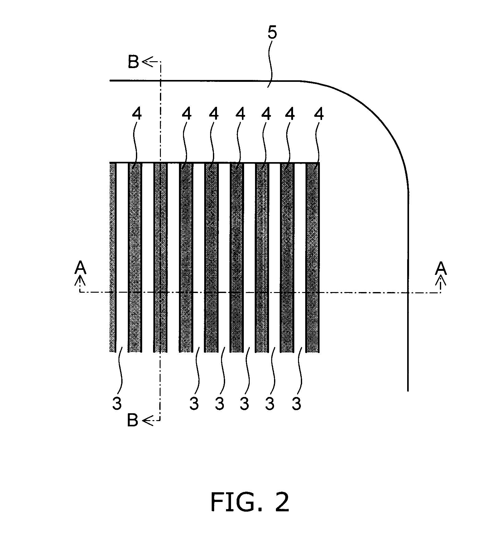
[0071]FIG. 2 is a schematic view showing an example planar pattern of pillar regions in the semiconductor device according to this embodiment.

[0072] Here, FIG. 1 shows the A-A cross section in FIG. 2.

[0073] On a major surface of a semiconductor layer (drain layer) 2 of highly doped n+-type silicon, first semiconductor pillar regions 3 of n-type silicon (hereinafter also simply referred to as “n-type pillar regions”) and second semiconductor pillar regions 4 of p-type silicon (hereinafter also simply referred to as “p-type pillar regions”) are periodically arranged in a direction substantially parallel to the major surface of the semiconductor layer 2. As shown in FIG. 2, the planar pattern of the n-type pillar regions 3 and the p-type pillar regions 4 has a striped configuration, for example.

[0074] The n-type pill...

second embodiment

[0100]FIG. 9A is a schematic view illustrating the cross-sectional structure of the main part of a semiconductor device according to a second embodiment of the invention, and FIG. 9B is a schematic diagram showing horizontal variation (variation along the direction from the device central region toward the edge termination section) in dopant concentration in the pillar regions shown in FIG. 9A. The vertical axis in FIG. 9B represents the dopant concentration in the pillar region.

[0101] In the embodiment shown in FIG. 9, the dopant concentration in the n-type pillar region 3 and the p-type pillar region 4 in the boundary region having stepwise varied depth is lower than the dopant concentration in the n-type pillar region 3 and the p-type pillar region 4 in the device central region (main cell section). By the stepwise varied depth of the n-type pillar region 3 and the p-type pillar region 4, the portion with no pillar region neighboring on one side is localized. Hence the breakdown...

third embodiment

[0106]FIG. 12 is a schematic view illustrating the opening pattern of a pillar region formation mask for the semiconductor device according to a third embodiment of the invention.

[0107]FIG. 13 is a schematic view illustrating dopants implanted into the C-C cross-sectional portion in FIG. 12.

[0108]FIG. 14 is a schematic view illustrating dopants implanted into the D-D cross-sectional portion in FIG. 12.

[0109]FIG. 15 is a schematic view illustrating dopants implanted into the E-E cross-sectional portion in FIG. 12.

[0110] The opening pattern of the pillar region formation mask shown in FIG. 12 is an example pattern for forming a superjunction structure in a striped configuration. A dopant for forming the p-type pillar region, e.g. boron 14, is implanted through the opening 17 of the p-type pillar region formation mask. A dopant for forming the n-type pillar region, e.g. phosphorus 15, is implanted through the opening 16 of the n-type pillar region formation mask.

[0111] By graduall...


PUM


Abstract

A semiconductor device includes: a semiconductor layer of a first conductivity type; a first semiconductor pillar region of the first conductivity type provided on a major surface of the semiconductor layer; a second semiconductor pillar region of a second conductivity type provided adjacent to the first semiconductor pillar region on the major surface of the semiconductor layer, the second semiconductor pillar region forming a periodic arrangement structure substantially parallel to the major surface of the semiconductor layer together with the first semiconductor pillar region; a first main electrode; a first semiconductor region of the second conductivity type; a second semiconductor region of the first conductivity type; a second main electrode; a control electrode; and a high-resistance semiconductor layer provided on the semiconductor layer in an edge termination section surrounding the first semiconductor pillar region and the second semiconductor pillar region. The high-resistance semiconductor layer has a lower dopant concentration than the first semiconductor pillar region. A boundary region is provided between a device central region and the edge termination section. The first semiconductor pillar region and the second semiconductor pillar region adjacent to the high-resistance semiconductor layer in the boundary region have a depth decreasing stepwise toward the edge termination section.

Description

CROSS-REFERENCE TO RELATED APPLICATIONS [0001] This application is based upon and claims the benefit of priorities from the prior Japanese Patent Applications No. 2006-137050, filed on May 16, 2006, No. 2006-170689, filed on Jun. 20, 2006, and No. 2007-100460, filed on Apr. 6, 2007; the entire contents of which are incorporated herein by reference. BACKGROUND OF THE INVENTION [0002] 1. Field of the Invention [0003] This invention relates to a semiconductor device, and more particularly to a semiconductor device suitable to power electronics and other applications. [0004] 2. Background Art [0005] The ON resistance of a vertical power MOSFET (Metal-Oxide-Semiconductor Field Effect Transistor) greatly depends on the electric resistance of its conduction layer (drift layer). The dopant concentration that determines the electric resistance of the drift layer cannot exceed a maximum limit, which depends on the breakdown voltage of a p-n junction formed by the base and the drift layer. Thu...

Claims


Application Information

Patent Timeline
Patent Type & Authority Applications(United States)
IPC IPC(8): H01L29/76
CPCH01L29/0619H01L29/872H01L29/0634H01L29/0696H01L29/0878H01L29/402H01L29/404H01L29/41741H01L29/7395H01L29/7397H01L29/7722H01L29/7806H01L29/7811H01L29/8611H01L29/0623
Inventor SAITO, WATARUONO, SYOTAROTAKASHITA, MASAKATSUSUMI, YASUTOIZUMISAWA, MASARUOHTA, HIROSHISEKINE, WATARU
Owner KK TOSHIBA
Why Eureka
Try Eureka