Mask forming and implanting methods using implant stopping layer and mask so formed

a technology of mask and stop layer, applied in the direction of thin material processing, electrical equipment, transportation and packaging, etc., can solve the problems of reducing the efficiency of the device, affecting the performance of the device, and affecting the effect of the effect of the device, so as to reduce scattering, the effect of reducing the aspect ratio of the mask and reducing the scattering

Inactive Publication Date: 2007-11-29
ALSEPHINA INNOVATIONS INC
View PDF7 Cites 6 Cited by
  • Summary
  • Abstract
  • Description
  • Claims
  • Application Information

AI Technical Summary

Benefits of technology

[0007]Methods of forming a mask for implanting a substrate and implanting using an implant stopping layer with a photoresist provide lower aspect ratio masks that cause minimal damage to trench isolations in the substrate during removal of the mask. In one embodiment, a method of forming a mask includes: depositing an implant stopping layer over the substrate; depositing a photoresist over the implant stopping layer, the implant stopping layer having a density greater than the photoresist; forming a patt...

Problems solved by technology

In the semiconductor fabrication industry continual miniaturization of structures presents challenges relative to modifying current techniques.
One challenge is addressing problems related to photolithography.
These patterned single layer photoresists have a relatively high aspect ratio, i.e., patterned photoresist height to pa...

Method used


Image

  • Mask forming and implanting methods using implant stopping layer and mask so formed
  • Mask forming and implanting methods using implant stopping layer and mask so formed
  • Mask forming and implanting methods using implant stopping layer and mask so formed

Examples


Embodiment Construction

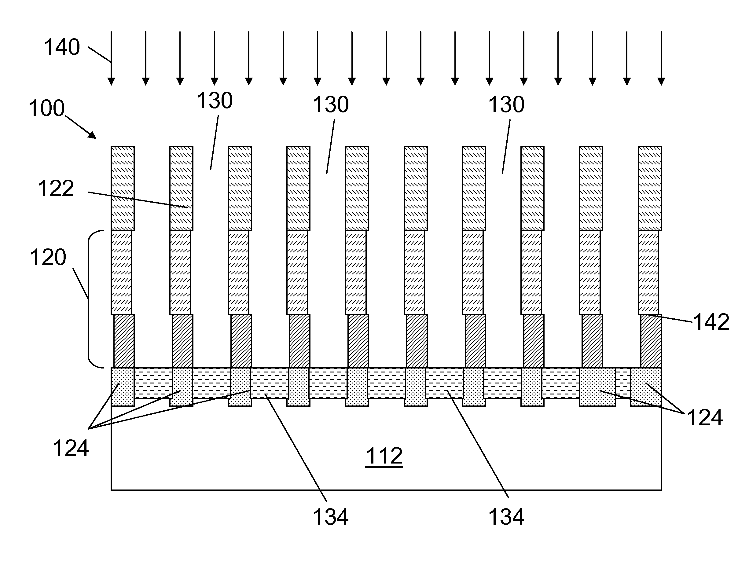
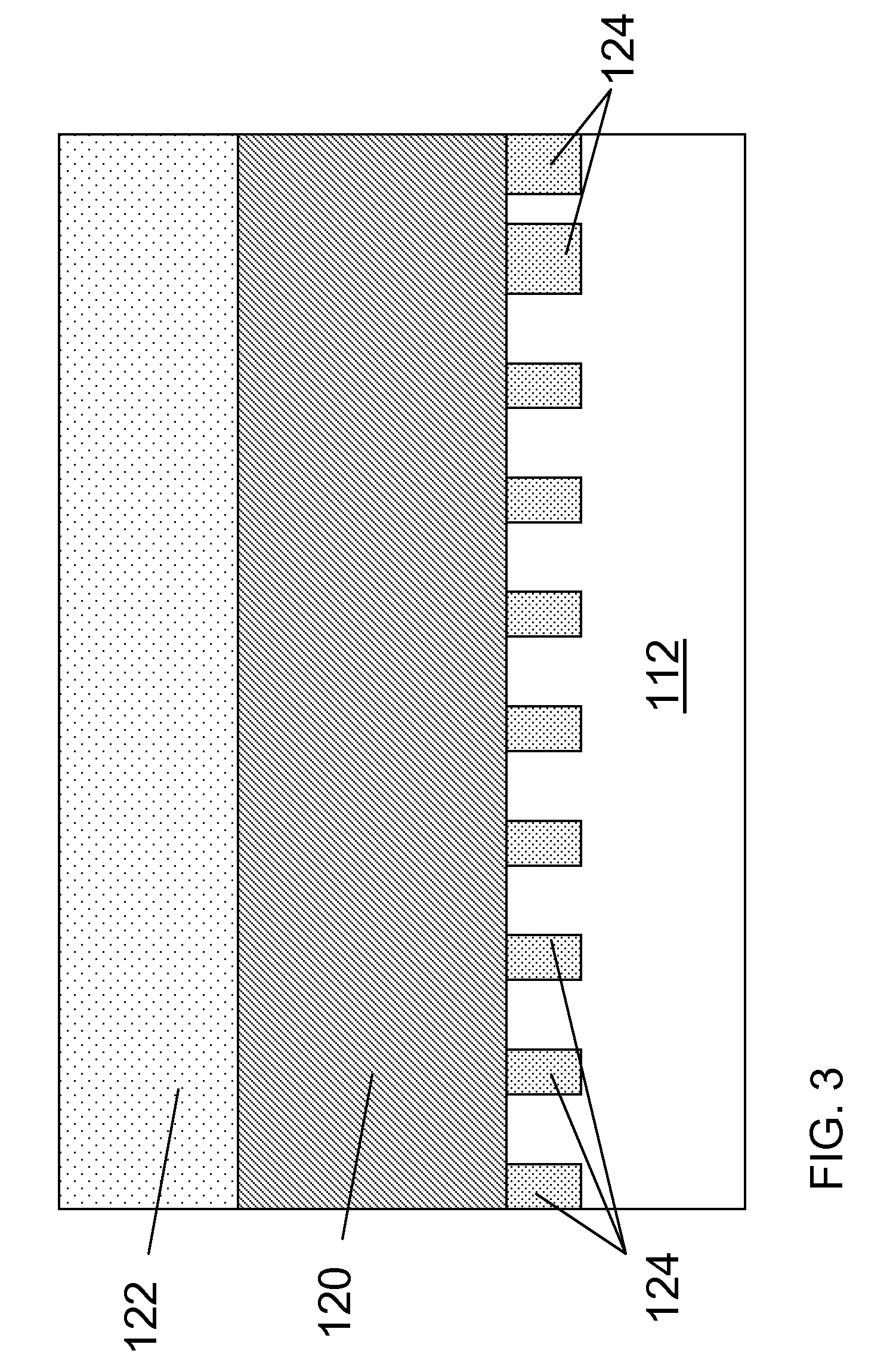
[0018]Turning to FIGS. 3-5, one embodiment of a method of forming a mask 100 (FIG. 5) for implanting a substrate 112 is illustrated. As shown in FIG. 3, a first step includes depositing an implant stopping layer 120 over substrate 112, followed by deposition of a photoresist 122 over implant stopping layer 120. Each layer may be deposited using any now known or later developed process. In one embodiment, however, ion implant stopping layer 120 is deposited by at least one of: chemical vapor deposition (CVD), low-pressure CVD (LPCVD), plasma-enhanced CVD (PECVD), semi-atmosphere CVD (SACVD) and high density plasma CVD (HDPCVD), rapid thermal CVD (RTCVD), ultra-high vacuum CVD (UHVCVD), sputtering deposition, ion beam deposition, electron beam deposition, and laser assisted deposition. Implant stopping layer 120 may have a depth that is greater than a depth of photoresist 122. Substrate 112 may include any now known or later developed substrate material such as one or more of the foll...


PUM


Abstract

Methods of forming a mask for implanting a substrate and implanting using an implant stopping layer with a photoresist provide lower aspect ratio masks that cause minimal damage to trench isolations in the substrate during removal of the mask. In one embodiment, a method of forming a mask includes: depositing an implant stopping layer over the substrate; depositing a photoresist over the implant stopping layer, the implant stopping layer having a density greater than the photoresist; forming a pattern in the photoresist by removing a portion of the photoresist to expose the implant stopping layer; and transferring the pattern into the implant stopping layer by etching to form the mask. The implant stopping layer may include: hydrogenated germanium carbide, nitrogenated germanium carbide, fluorinated germanium carbide, and/or amorphous germanium carbon hydride (GeHX), where X includes carbon. The methods/mask reduce scattering during implanting because the mask has higher density than conventional masks.

Description

BACKGROUND OF THE INVENTION[0001]1. Technical Field[0002]The invention relates generally to semiconductor device fabrication, and more particularly, to a method for forming a mask for implanting a substrate, where the mask includes an implant stopping layer, and a mask so formed.[0003]2. Background Art[0004]In the semiconductor fabrication industry continual miniaturization of structures presents challenges relative to modifying current techniques. One challenge is addressing problems related to photolithography. Photolithography is a process used in the semiconductor fabrication industry in which a photo-sensitive material, i.e., a photoresist, is laid upon a substrate, imaged and then etched to leave a pattern that can be used to generate other structures within the substrate. As miniaturization continues, the dimensions of patterned photoresists are also being minimized. Some processing, for example, deep well ion implants, require very thick layers of photoresist to block ion im...

Claims


Application Information

Patent Timeline
IPC IPC(8): H01L21/302H01L21/461
CPCH01L21/26513Y10T428/24992H01L21/266
Inventor BABICH, KATHERINABAILEY, TODD C.CONTI, RICHARD A.DESCHNER, RYAN P.
Owner ALSEPHINA INNOVATIONS INC
Why Eureka
Try Eureka