Rf Tags

a technology of rf tags and substrates, applied in the field of rf tags, can solve the problems of requiring a costly further processing step, affecting the quality of rf tags, and requiring a costly further production step, so as to achieve the effect of increasing the number of substrate materials, reducing the cost of further processing, and reducing the cost of further production

Inactive Publication Date: 2007-12-13
QINETIQ LTD
View PDF18 Cites 3 Cited by
  • Summary
  • Abstract
  • Description
  • Claims
  • Application Information

AI Technical Summary

Benefits of technology

[0018] Alternatively, the dielectric may be deposited directly onto the substrate substantially in the pattern of the circuit, by any known pattern transfer mechanism. Conveniently the dielectric may be in the form of a printable ink, which may be deposited by known means. The advantage of depositing the dielectric layer, rather than using the substrate as the dielectric, is that there are an increased number of substrate materials which are available to use. In the manufacture of prior art RF tags the substrates are selected to be rugged, to sufficiently support the circuit and also act as a dielectric. Therefore cheaper and / or more rugged materials may be selected for use as substrates.
[0019] Therefore a dielectric may be selected which possesses a low dissipation factor. A further advantage of depositing a dielectric layer comes from the reduced thickness of a deposited or printed dielectric layer compared to the typical thickness of a substrate. The reduction in thickness of the dielectric increases the capacitance value of the deposited capacitor. Therefore this enables capacitor plates with reduced areas to be used to achieve the same values of capacitance. This may lead to a decrease in the overall area of the RF tag.

Problems solved by technology

This requires a costly further processing step of aligning and folding the substrate to co-locate the respective capacitor plates.
Such a folding step is likely to cause stress to the metal on the surface of the substrate.
The conducting bridge must be prepared in a separate process step, and in order to function it is required to contain electrically conducting regions and electrically insulated regions This requires a costly further production step of the bridging portions, and also further alignment and fixing process steps.
Whilst this cleverly utilises the materials it also adds to process complexity and cost by having to process both sides of the substrate.

Method used


Image

  • Rf Tags
  • Rf Tags

Examples


example 1

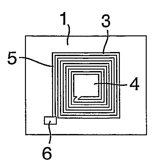
[0067] A screen printing ink (supplied under the trade mark Acheson 6018S) was used as the ink formulation, to which was added titanium dioxide 2 μm at 30% by weight as a filler and silver nitrate 3% by weight. The silver nitrate was pre-dissolved in an aliquot of ethyl lactate / water to aid the transfer and mixing with the screen printing ink. The ink composition was screen printed onto one side of a sheet of polyester in the design of a “checkpoint®” system electronic article surveillance, (EAS), 1-bit tag.

[0068] The ink was cured by heating the sample to 80° C. for 10 minutes, causing the ink composition to solidify and adhere to the substrate. At this stage the ink had no electrical conductivity. The printed pattern of cured ink was then immersed into a solution of commercially available Enthone 2130® electroless copper at 46° C. and copper metal deposited to a thickness in the range of from 0.1 to 2 microns onto the printed pattern. An effective EAS tag requires greater than 2 ...

examples 2-4

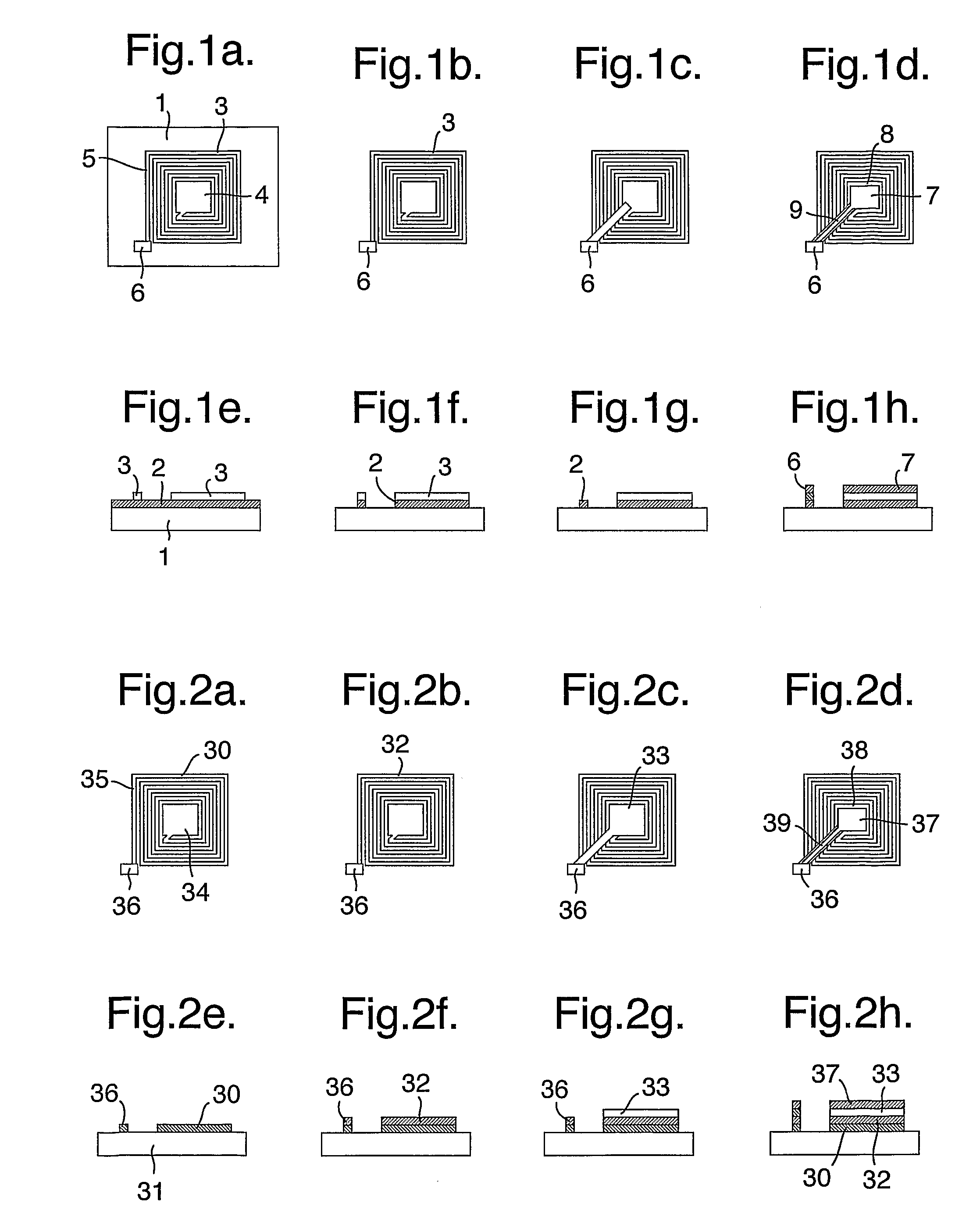
[0071] In the examples a compound of tin SnCl2.2H2O was dissolved into ethyl lactate to form an ink formulation of concentration in the range 1-100 millimolar (preferably 2-20 millimolar). Three varieties of this ink formulation were prepared. Example 2 used an inkjet formulation simply using the above prepared solution. Example 3 used an inkjet formulation that additionally comprised an additional 1% by weight ethyl cellulose binder. Both of these inks were printed onto a polyester substrate in the pattern of a first conducting layer of an RF circuit, as shown FIG. 2.

[0072] Example 4 used an ink which was prepared by adding the ink formulation to a commercial screen printing ink (the TiO2 based formulation 6018S from Acheson). Additions in the range 1-100 ml of the ink formulation (preferably 10-30 ml) were added to 100 grams of the screen printing paste and mixed in. This screen printing ink formulation was printed onto a polyester substrate and dried at 60° C. for 1 hour.

[0073]...


PUM

PropertyMeasurementUnit
thicknessaaaaaaaaaa
thicknessaaaaaaaaaa
thicknessaaaaaaaaaa

Abstract

A single sided RF tag suitable for use for electronic article surveillance comprises a tuned circuit formed on one side of a substrate. Provided by a deposited first conducting layer which comprises an inductive coil, which behaves as an antenna and is electrically connected to a first capacitor plate and a connection means to connect to a second conducting layer. A low dissipation factor dielectric layer is deposited onto said first conducting layer. A second conducting layer comprising at least one capacitor and a connection means to electrically connect to the first conducting layer is deposited on the dielectric layer. The second capacitor plate is substantially co-located above the first capacitor plate, to form the capacitor. The capacitor and coil together form a resonant circuit. The circuit pattern for the first and second layer may be formed by known metal printing techniques, such as, for example the use of a catalytic seed layer which is deposited by a pattern transfer mechanism into the circuit pattern. Alternatively the circuit pattern may be formed by standard photo-lithography etch techniques to reveal a circuit pattern from a metallised surface. The tag will preferably incorporate known methods of fusing to deactivate or detune the tag, to permit removal of articles from an enclosed area. The substrate may further include a second RF tag tuned to an alternative frequency on the opposite side of the substrate. Alternatively a plurality of tags may be built up in successive layers on one or both sides of the tag.

Description

[0001] The invention relates to radio-frequency (RF) tags which are capable of being detected by an external electric field and in particular to RF tags which can be formed on a single side of a substrate. Such tags are frequently used for Electronic Article Surveillance (EAS) to detect unauthorised articles being removed from enclosed areas such shops or libraries. [0002] One bit RF tags typically comprise a tuned circuit having inductive and capacitor components. A “gate” is arranged at the exit to the enclosed area and coils within the gate generate an electrical field at the resonant frequency of the tag. If the tag passes through the gate the field is disrupted and circuitry attached to the gate detects this disruption and generates a signal which may trigger an alarm. In practice the gate frequency commonly scans frequencies around the expected resonant frequency to allow for manufacturing variation in the tag. [0003] To permit authorised removal the tag is de-activated. For e...

Claims


Application Information

Patent Timeline
Patent Type & Authority Applications(United States)
IPC IPC(8): G08B13/24
CPCG08B13/2414Y10T29/49002G08B13/2437G08B13/242G08B13/24
Inventor JOHNSON, DANIELR
Owner QINETIQ LTD
Why Eureka
Try Eureka