
Bipolar Semiconductor Device and Process for Producing the Same

a semiconductor device and bipolar technology, applied in the direction of semiconductor devices, electrical appliances, transistors, etc., can solve the problems of degrading the reliability of a power conversion device, increasing the loss, and degrading the forward voltage, so as to achieve the effect of propagating a basal plane dislocation and greatly reducing the dislocation of an epitaxial layer

Inactive Publication Date: 2007-12-20
THE KANSAI ELECTRIC POWER CO +1
View PDF5 Cites 62 Cited by
  • Summary
  • Abstract
  • Description
  • Claims
  • Application Information

AI Technical Summary

Benefits of technology

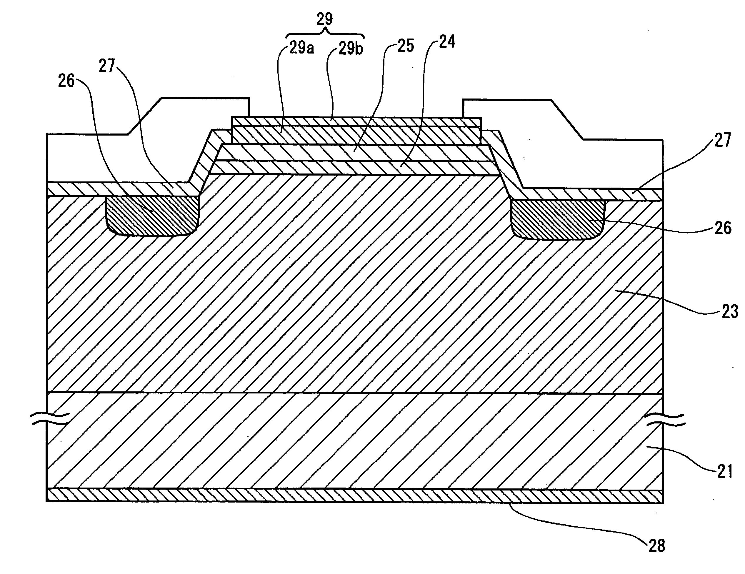
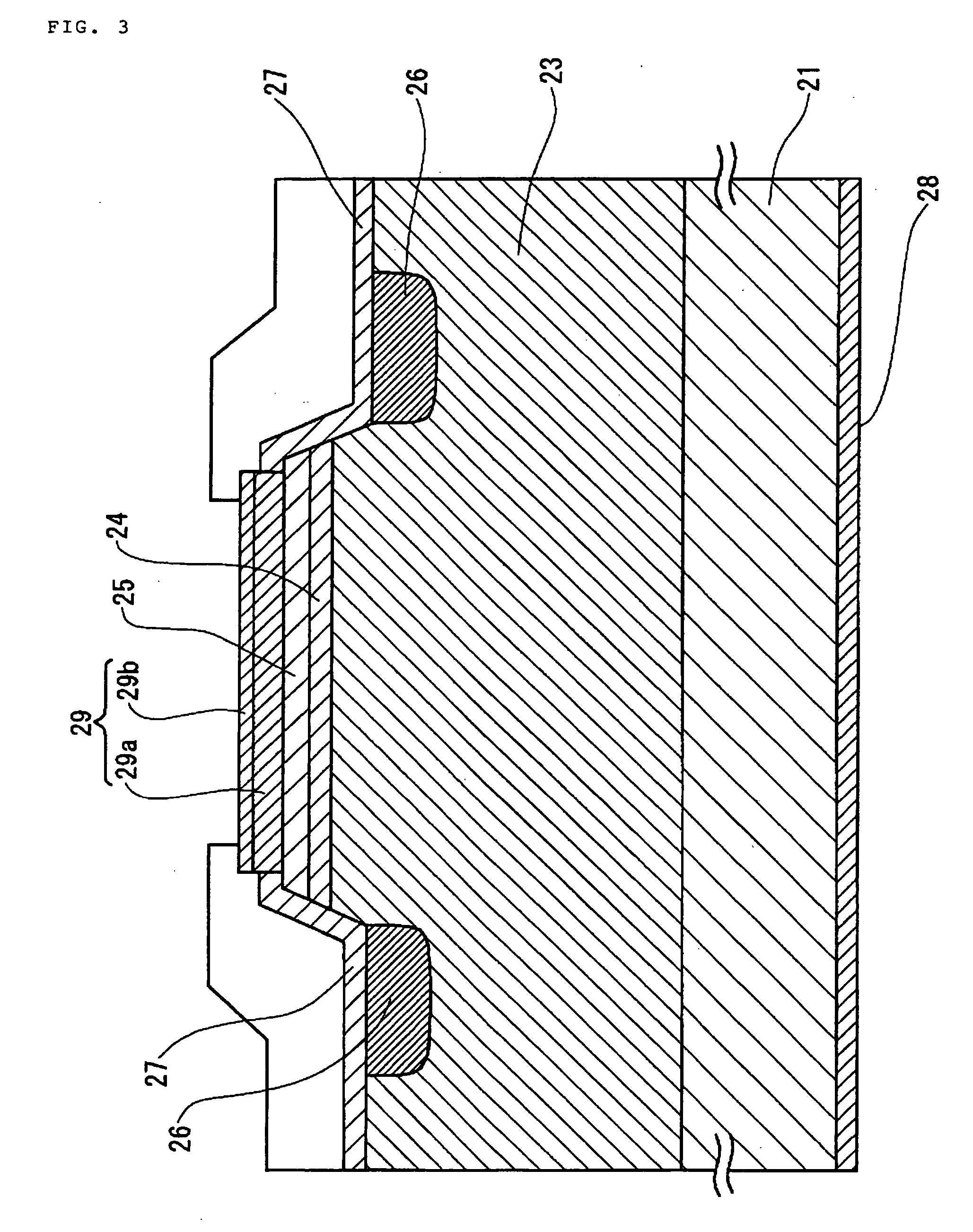
[0024] According to a bipolar type semiconductor device related to the present invention, a basal plane dislocation in an epitaxial layer can be greatly reduced.
[0025] According to the manufacturing process of a bipolar type semiconductor device related to the present invention, the propagation of a basal plane dislocation from an SiC monocrystal substrate to an epitaxial layer can be greatly reduced.

Problems solved by technology

It is thought that such degradation of a forward voltage is caused by a basal plane dislocation, which is a kind of crystal faults.
In the case in which a forward voltage is increased, a loss of an device increases, thus increasing a loss and degrading the reliability for a power conversion device such as an inverter using such an device.
In the case in which a power semiconductor device is formed with SiC monocrystal, deep diffusion of impurities is difficult since a diffusion coefficient of the SiC monocrystal is extremely small.

Method used

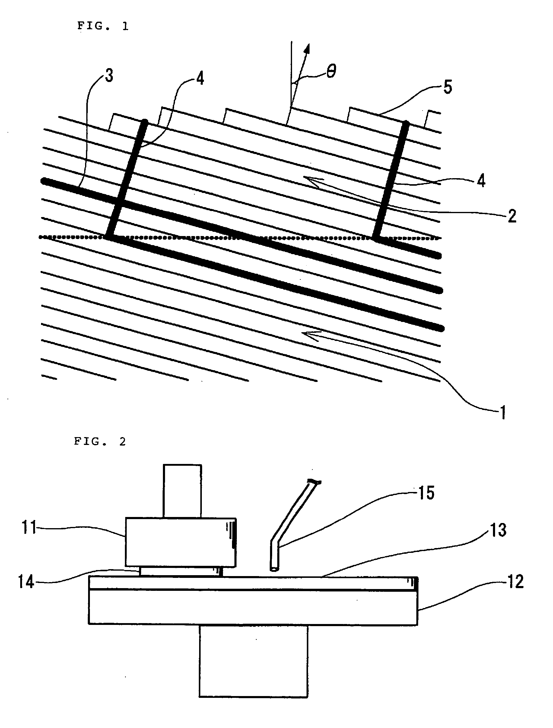

Image

  • Bipolar Semiconductor Device and Process for Producing the Same
  • Bipolar Semiconductor Device and Process for Producing the Same
  • Bipolar Semiconductor Device and Process for Producing the Same

Examples


example 1

[0091] An ingot that was grown by an modified Lely method was sliced at an off-angle of 8° to the off-orientation of the [11-20] direction. The surface of the sliced substrate was smoothed in the specular morphology by mechanically polishing the surface with abrasive grains. By using a vertical type hot wall reactor, an etching treatment for 40 minutes was carried out at a temperature of 1400° C. and a pressure of 30 Torr to the formed n-type 4H—SiC (0001) substrate while supplying a hydrogen gas at a flow rate of 10 L / min. The surface roughness Rms of the substrate, which was measured by using the interatomic force microscope SPI3800N manufactured by Seiko Instruments Inc. after the treatment, was 0.25 nm (region of 10 μm×10 μm).

[0092] Next, the epitaxial growth of SiC from the surface of the substrate was carried out by the CVD method after the treatment. An epitaxial film with a film thickness of 60 μm was formed by the step flow growth for 4 hours at a temperature of 1545° C. a...

example 2

[0094] The SiC monocrystal substrate with the epitaxial film was obtained similarly to the Example 1 except that the surface of the substrate was treated by chemical mechanical polishing before carrying out a hydrogen etching treatment. The surface roughness Rms of the substrate, which was measured based on the method same as that of the Example 1 after the treatment, was 0.20 nm (region of 10 μm×10 μm).

[0095] The basal plane dislocation density in the epitaxial film, which was measured by using the molten KOH etching and X-ray topograph for the SiC monocrystal substrate with the epitaxial film that was obtained, was 60 cm−2 on the average.

example 3

[0096] An ingot that was grown by an modified Lely method was sliced at an off-angle of 8° to the off-orientation of the [11-20] direction. The surface of the sliced substrate was smoothed in the specular morphology by mechanically polishing the surface with abrasive grains. The formed n-type 4H—SiC (000-1) substrate was treated by chemical mechanical polishing and hydrogen etching and then an epitaxial film was grown similarly to the Example 2. The surface roughness Rms of the substrate, which was measured based on the method same as that of the embodiment 1 after the treatment, was 0.20 nm (region of 10 μm×10 μm).

[0097] The basal plane dislocation density in the epitaxial film, which was measured by using the molten KOH etching and X-ray topograph for the SiC monocrystal substrate with the epitaxial film that was obtained, was 20 cm−2 on the average.


PUM

PropertyMeasurementUnit
surface roughness Rmsaaaaaaaaaa
off-angleaaaaaaaaaa
off-angleaaaaaaaaaa

Abstract

A process for manufacturing a bipolar type semiconductor device in which at least a part of a region where an electron and a hole are recombined during current flowing is formed with a silicon carbide epitaxial layer that has been grown from the surface of a silicon carbide substrate, is characterized by that the surface of the silicon carbide substrate is treated by hydrogen etching and the epitaxial layer is then formed by the epitaxial growth of silicon carbide from the treated surface. A propagation of a basal plane dislocation to the epitaxial layer can be further reduced by treating the surface of the silicon carbide substrate by using chemical mechanical polishing and hydrogen etching in this order.

Description

TECHNICAL FIELD [0001] The present invention relates to a bipolar type semiconductor device and its manufacturing process in which a region where an electron and a positive hole are recombined during current flowing, such as a drift layer, is formed with a silicon carbide epitaxial layer that has been grown from the surface of a silicon carbide substrate, in particular to a reduction of a basal plane dislocation density in the epitaxial layer and an improvement of a forward voltage degradation due to long-term operation. BACKGROUND ART [0002] Silicon carbide (SiC) is a semiconductor that has excellent material property values for a coefficient of thermal conductivity, electron mobility, and a band gap, in addition to the dielectric breakdown field strength of approximately ten times as strong as that of silicon (Si). Accordingly, silicon carbide is expected as a semiconductor material for implementing rapid performance improvement as compared with conventional Si power semiconductor...

Claims


Application Information

Patent Timeline
Patent Type & Authority Applications(United States)
IPC IPC(8): H01L21/20H01L21/205H01L21/302H01L21/331H01L21/336H01L29/73H01L29/78H01L29/861H01L21/04H01L29/737H01L29/74
CPCH01L21/02019H01L21/02024H01L29/8613H01L21/0262H01L21/02378H01L21/02433H01L21/02529H01L21/02661
Inventor NAKAYAMA, KOJISUGAWARA, YOSHITAKATSUCHIDA, HIDEKAZUKAMATA, ISAHOMIYANAGI, TOSHIYUKINAKAMURA, TOMONORI
Owner THE KANSAI ELECTRIC POWER CO
Learn More