

NANO imprint technique with increased flexibility with respect to alignment and feature shaping
a technology of feature shaping and imprinting, which is applied in the field of microstructure fabrication, can solve the problems of high burden on tool manufacturers, uncertainty in overlaying the image of the pattern for the current material layer, and variations of etched features, so as to reduce the number of process steps, reduce the complexity of imprinting techniques, and improve the degree of flexibility
- Summary
- Abstract
- Description
- Claims
- Application Information
AI Technical Summary
Benefits of technology
Problems solved by technology
Method used
Image

Examples
Embodiment Construction
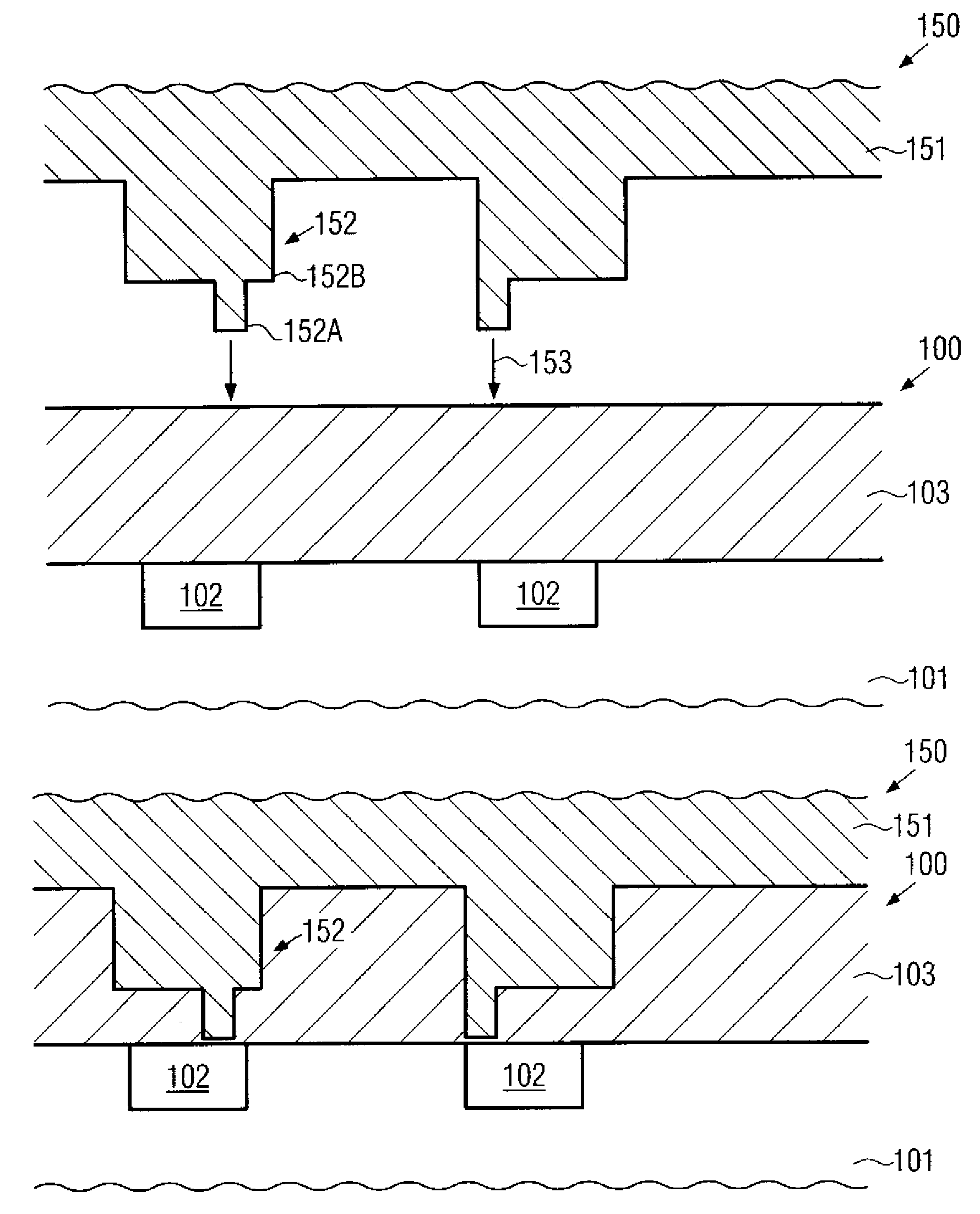
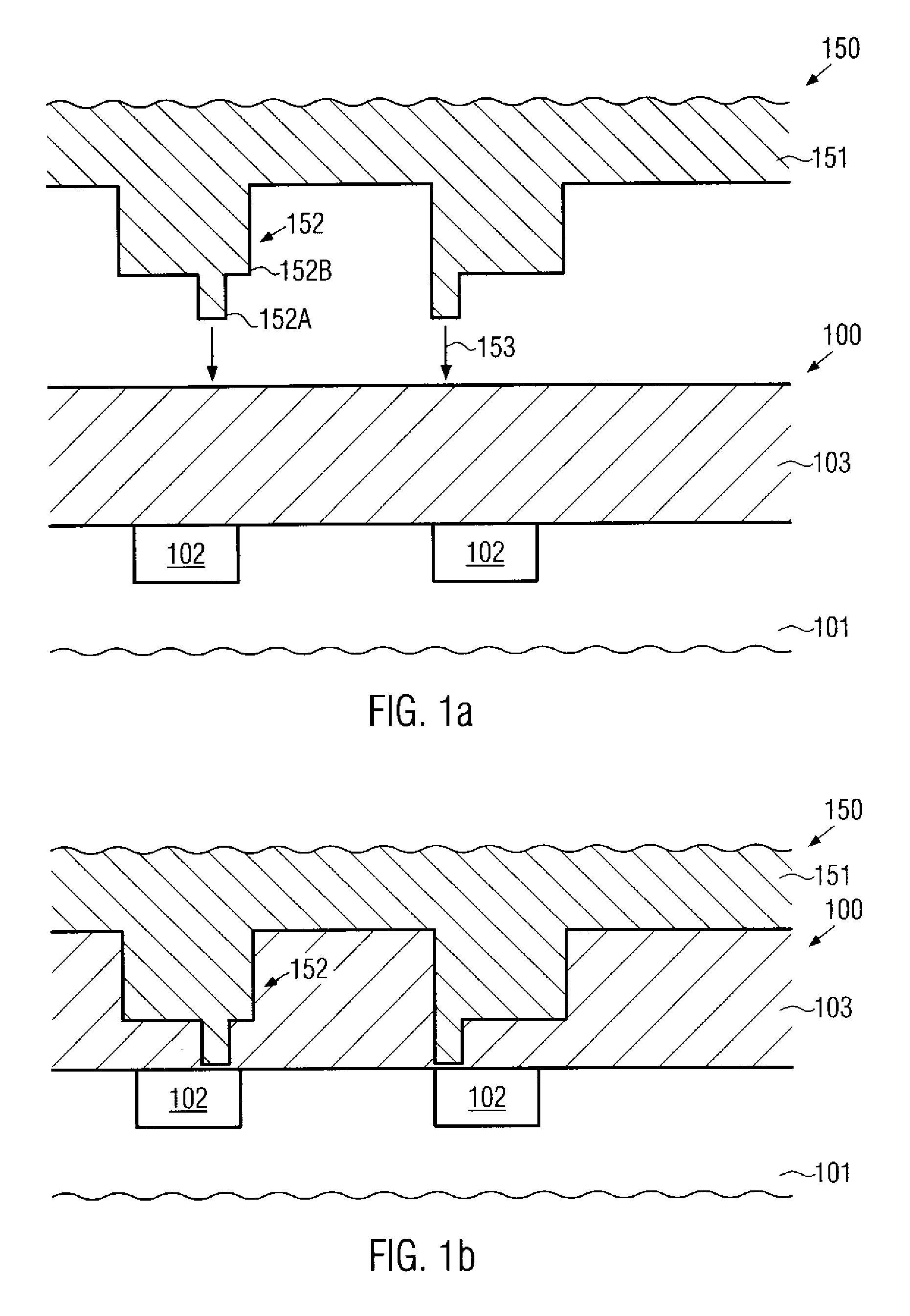
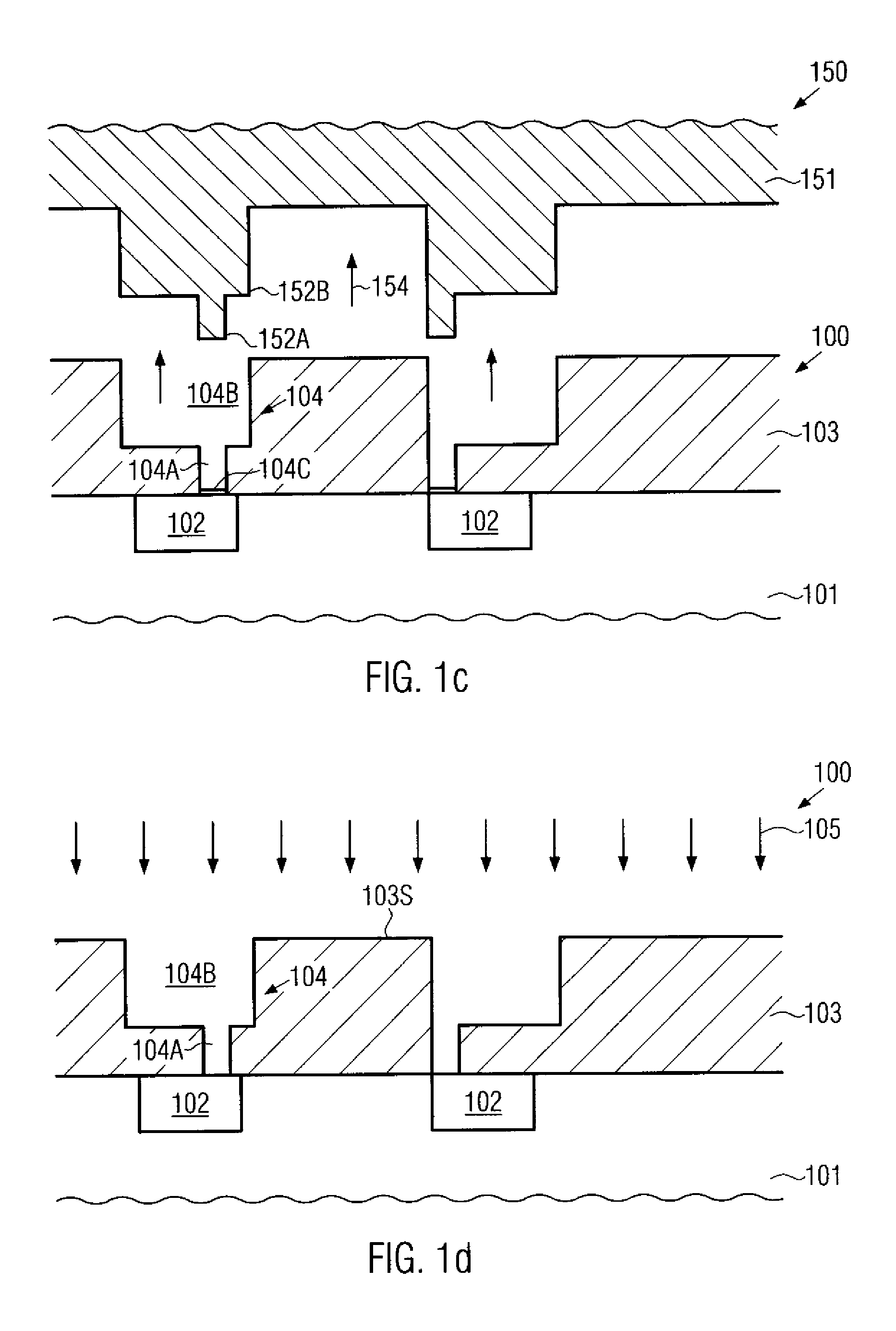
[0024] Various illustrative embodiments of the invention are described below. In the interest of clarity, not all features of an actual implementation are described in this specification. It will of course be appreciated that in the development of any such actual embodiment, numerous implementation-specific decisions must be made to achieve the developers' specific goals, such as compliance with system-related and business-related constraints, which will vary from one implementation to another. Moreover, it will be appreciated that such a development effort might be complex and time-consuming, but would nevertheless be a routine undertaking for those of ordinary skill in the art having the benefit of this disclosure.
[0025] The present subject matter will now be described with reference to the attached figures. Various structures, systems and devices are schematically depicted in the drawings for purposes of explanation only and so as to not obscure the present disclosure with detai...
PUM
 Abstract
Description
Claims
Application Information