Plasma etching method and computer-readable storage medium

a technology of etching method and etching method, which is applied in the field of plasma etc., can solve the problems of enlargement of openings, low plasma resistance of photoresist, and surface roughening, and achieve the effect of increasing the plasma resistance of the hard mask layer, sufficient etching selectivity, and improving etching selectivity

Active Publication Date: 2008-01-24
TOKYO ELECTRON LTD
View PDF7 Cites 18 Cited by
  • Summary
  • Abstract
  • Description
  • Claims
  • Application Information

AI Technical Summary

Benefits of technology

[0015]In accordance with the present invention, since a plasma etching is performed on a substrate, on which an oxide film as a target layer to be etched, a hard mask layer and a patterned photoresist are sequentially formed, by a processing gas including CxFy (x is an integer equal to or less than 3, y is an integer equal to or less than 8), C4F8, a rare gas and O2, it is possible to form holes of fine etching shapes without bowing or the like at a practical etching rate, even if the holes have a high aspect ratio of a narrow width. Further, in a conventional process using the above processing gas system, a sufficient etching se

Problems solved by technology

Since, however, the ArF photoresist has a low plasma resistance, it suffers a surface roughening during an etching, which hardly occurs when using the KrF photoresist.
Accordingly, there occur such problems of a formation of longitudinal strips (striation) on inner wall surfaces of openings, enlargements of openings (i.e., an increase of critical dimension (CD)), and the like.

Method used


Image

  • Plasma etching method and computer-readable storage medium
  • Plasma etching method and computer-readable storage medium
  • Plasma etching method and computer-readable storage medium

Examples


first embodiment

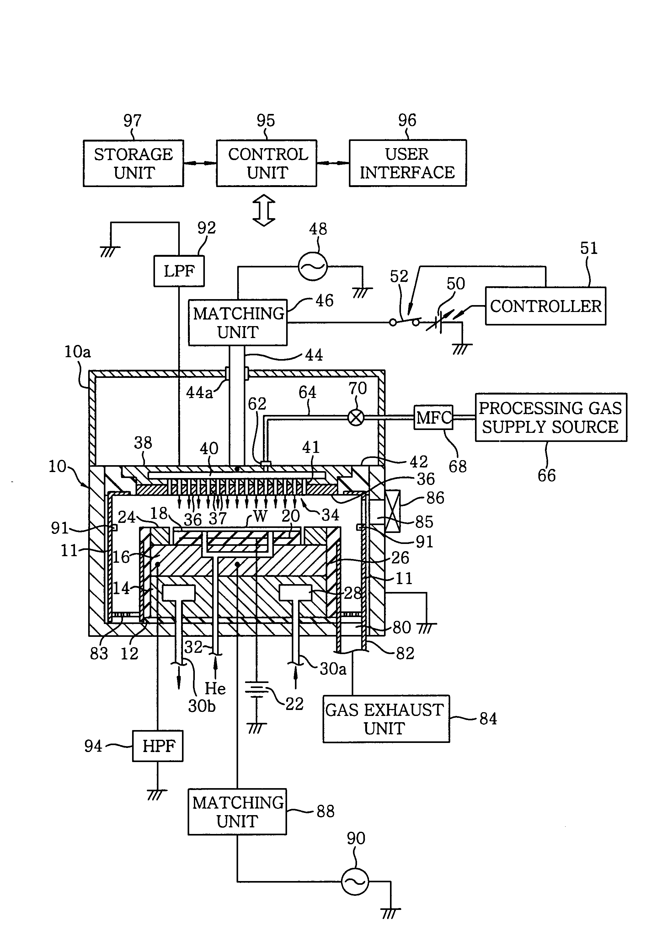
[0053]Hereinafter, there will be described a plasma etching method in accordance with the present invention, which is performed by the plasma etching apparatus having the aforementioned configuration.

[0054]Referring to FIG. 3, a semiconductor wafer W to be processed has an etching stop film 102, an oxide film 103 as a target layer to be etched, a hard mask layer 104, a bottom anti-reflection coating (BARC) film 105 and a photoresist film 106 that are sequentially formed on a Si substrate 101, wherein the photoresist film is provided with a certain pattern. The hard mask layer 104 is first etched by using the photoresist film 106 as a mask, and the oxide film 103 which is a target layer is then etched.

[0055]In this embodiment, the oxide film 103 can be formed of, e.g., tetraethoxysilane (TEOS), a glass film (BPSG or PSG) or the like. The thickness of the oxide film 103 is appropriately set, and, for example, when it is used as a DRAM capacitor, its thickness is set to be in a range f...

experiment 1

[0076](Experiment 1)

[0077]A sample used in this experiment was fabricated to have a structure shown in FIG. 3, by sequentially forming, on a Si substrate, a SiN film having a thickness of 50 nm as an etching stop film 102, a two-layered film formed of a BPSG film (lower layer) and a TEOS film (upper layer) having a thickness 1500 nm as a target oxide film 103 to be etched, an amorphous carbon film having a thickness of 500 nm as a hard mask layer 104, a SiON film having a thickness of 60 nm as a bottom anti-reflection coating (BARC) film 105, and an ArF resist having a thickness of 200 nm as a photoresist film 106. After etching the hard mask layer 104 by using the apparatus shown in FIG. 1, the oxide film 103 was etched under various conditions by using residues of the photoresist film 106 and the hard mask layer 104 as an etching mask. Here, etching of circular holes each having a diameter of 90 nm was performed.

[0078]For the etching of the oxide film, processing conditions were a...

experiment 2

[0094](Experiment 2)

[0095]Here, a sample having the same structure as that of the Experiment 1 was fabricated, and after etching a hard mask layer 104 by using the apparatus shown in FIG. 1, an oxide film 103 was etched by using residues of a photoresist film 106 and the hard mask layer 104 as a mask. In this experiment, a processing pressure, an upper electrode temperature and a lower electrode temperature were maintained at 2.7 Pa, 95° C. and 10° C., respectively.

[0096]Further, in condition I, a high frequency power to the upper electrode and a high frequency power to the lower electrode were set to be 1200 W and 3800 W, respectively; a DC voltage was set to be −1000 V; and flow rates of C4F8, C3F8, Ar and O2 were set to be 40 mL / min (sccm), 25 mL / min (sccm), 900 mL / min (sccm) and 30 mL / min (sccm), respectively.

[0097]In condition J, the high frequency power to the upper electrode and the high frequency power to the lower electrode were set to be 1200 W and 3800 W, respectively; th...


PUM

PropertyMeasurementUnit
Electric potential / voltageaaaaaaaaaa
Widthaaaaaaaaaa
Flow rateaaaaaaaaaa

Abstract

In a plasma etching method, a substrate, on which an oxide film as a target layer to be etched, a hard mask layer, and a patterned photoresist are sequentially formed, is loaded into the processing chamber and mounted on a lower electrode. A processing gas containing CxFy (x is 3 or less and y is 8 or less), C4F8, a rare gas and O2 is supplied and a plasma of the processing gas is generated by applying a high frequency power to an upper or a lower electrode. Further, a high frequency power for bias is applied to the lower electrode, and a DC voltage is applied to the upper electrode.

Description

FIELD OF THE INVENTION [0001]The present invention relates to a plasma etching method for performing a plasma etching on an oxide film formed on a substrate through a mask layer, and a computer-readable storage medium for storing therein a control program to be used in executing the plasma etching method.BACKGROUND OF THE INVENTION [0002]In a manufacturing process of a semiconductor device, a photoresist pattern is formed on a semiconductor wafer, which is a substrate to be processed, through a photolithography process to be used as a mask in etching of the semiconductor wafer.[0003]With a recent trend of miniaturization of semiconductor devices, etching also requires microprocessing. To keep up with such trend of micro-etching, the thickness of a photoresist film used as a mask is getting thinner, and the kind of the photoresist is shifting from a KrF photoresist (i.e., a photoresist exposed to a laser beam of which an emission source is a KrF gas) to an ArF photoresist (i.e., a ph...

Claims


Application Information

Patent Timeline
IPC IPC(8): H01L21/3065
CPCH01L21/31116H01J37/32091
Inventor UEDA, KOSEISASAKI, HIKOICHIRO
Owner TOKYO ELECTRON LTD
Why Eureka
Try Eureka