
Method and apparatus for trans-zone sputtering

Inactive Publication Date: 2008-02-07
DORFMAN BENJAMIN F
View PDF3 Cites 8 Cited by
  • Summary
  • Abstract
  • Description
  • Claims
  • Application Information

AI Technical Summary

Benefits of technology

[0016]1. Trans-zone sputtering wherein the particles ejected from a sputter zone of anytreated material, condense backwards onto the deposition zone upon the surface of the same material from which these particles were ejected via sputtering. The useful effect is attained due to certain special properties of the deposited layer, especially in the case of polymer materials where the layer deposited from relatively high-energetic carbon-containing particles is enriched by sp(sup3), or covalent bonded carbon, also known as diamond-like carbon. Also the deposited layer is virtually free of nano-pores, and improves smoothness and tribological properties of the engineered surface.
[0030]Furthermore, the sputtering process automatically, by design, realizes the necessary surface preparation in situ in the sputter zone, prior to deposition in the deposition zone. As the result, the productivity of sputtering-deposition process is essentially higher than in prior art, the labor expenses are lower, and emission during the equipment cleaning dramatically decreases. Although the scope of applications of Trans-Zone Sputtering is confined to ultra-thin surface layers, it provides a powerful technological tool for many industries, and it makes the ion sputtering technique economically sound even in such application fields where it was not feasible based on prior art, such as the field of surface engineering in mass production for the plastic industry.

Problems solved by technology

Magnetron sputtering is a powerful alternative to less effective vacuum evaporation and extremely emissive and harmful electrochemical deposition.
This results in losses of valuable materials and produces undesirable side effects requiring time and labor expenditures and emission control measures.
On the other hand, the effectiveness of target use is not high as well.
This is due to the uneven profile of the sputtering rate along of the surface of the target, and because the target cannot be consumed beyond a certain percentage of its initial thickness, typically not exceeding about 50% of initial target thickness in the area of its maximum sputtering rate, because of mechanical requirements.
Furthermore, an uneven profile of the partially consumed target results with an uneven profile for the deposited layer as well, especially in the chamber geometry with a short distance between target and substrate; because of uneven profiles, the targets are often changed when only as little as 25% has been consumed.
The other innate problem of magnetron technique is the extremely high power density upon the surface of consumable target.
As a result, magnetron assemblies are heavy devices.
Not only does it increase the cost of production, installation and maintenance of the equipment, but it limits the possibility in optimizing the magnetron design, because the maximum sputter-deposition rate requires the target assembly having as thin a cross-section as possible.
In such a case, the substrate material subjected to cleaning serves as consumable target, while the sputtered matter deposited upon the inside walls of vacuum chamber is virtually lost.

Method used


Image

  • Method and apparatus for trans-zone sputtering
  • Method and apparatus for trans-zone sputtering
  • Method and apparatus for trans-zone sputtering

Examples


example 1

[0126]In the below example a 200-micrometer thick Teflon tape underwent surface engineering with the purpose to close superficial nano-pores in the typical diameter range of 1 nm to 4 nm. The engineering was conducted using a rectangular magnetron; the width of the sputter zone is 8″, and the sputtered and deposited layers are 10-nm thick. The power density is 10 W / cm (sup2), RF.

[0127]The distance between the tape and magnetron cathode is 2 mm.

[0128]Note: this 2-mm gap is designated for decreasing the heat exchange between the tape and magnetron cathode; the exact width of the gap is not critical, and even occasional touching between tape and cathode will not result in damage.

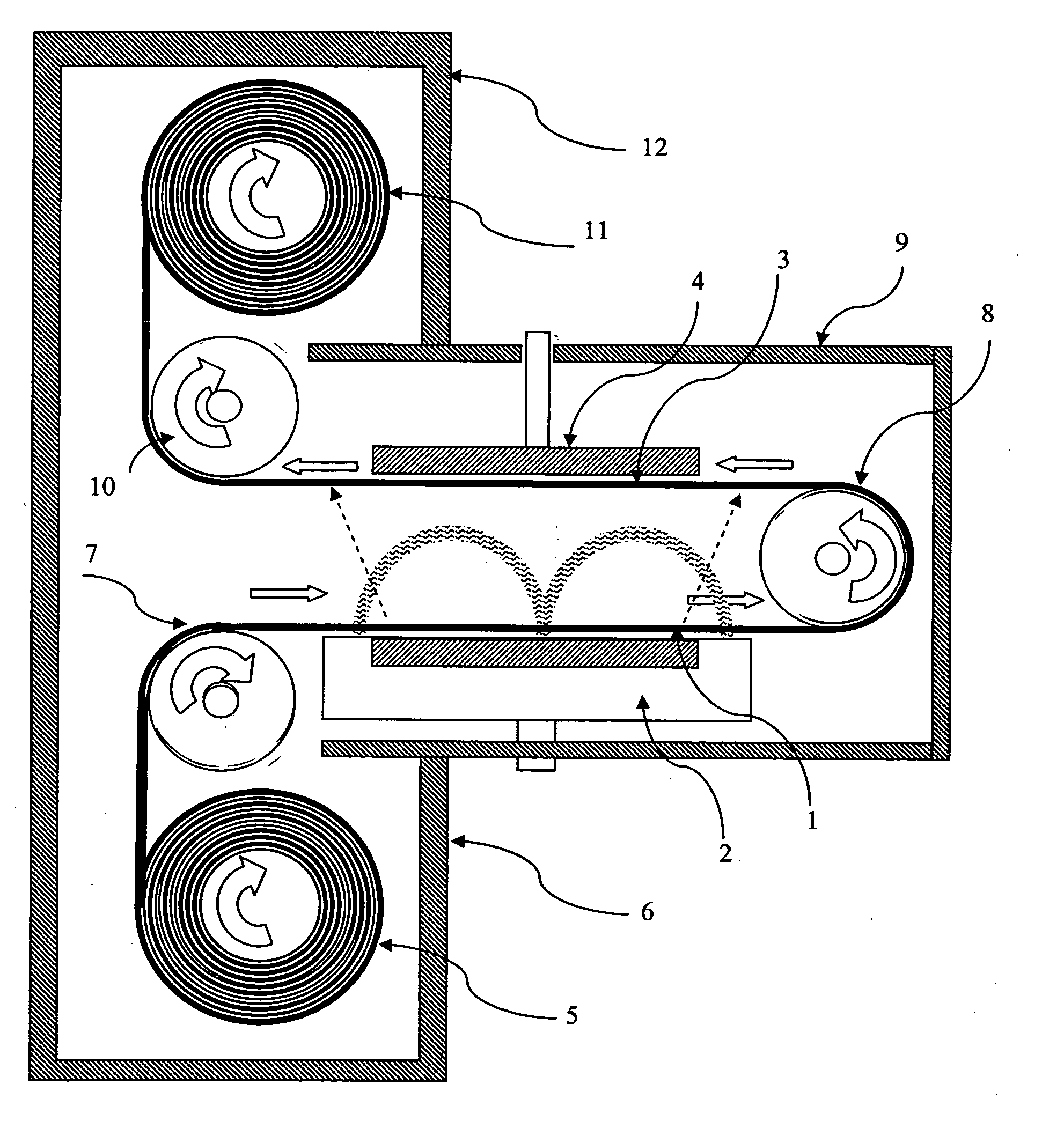
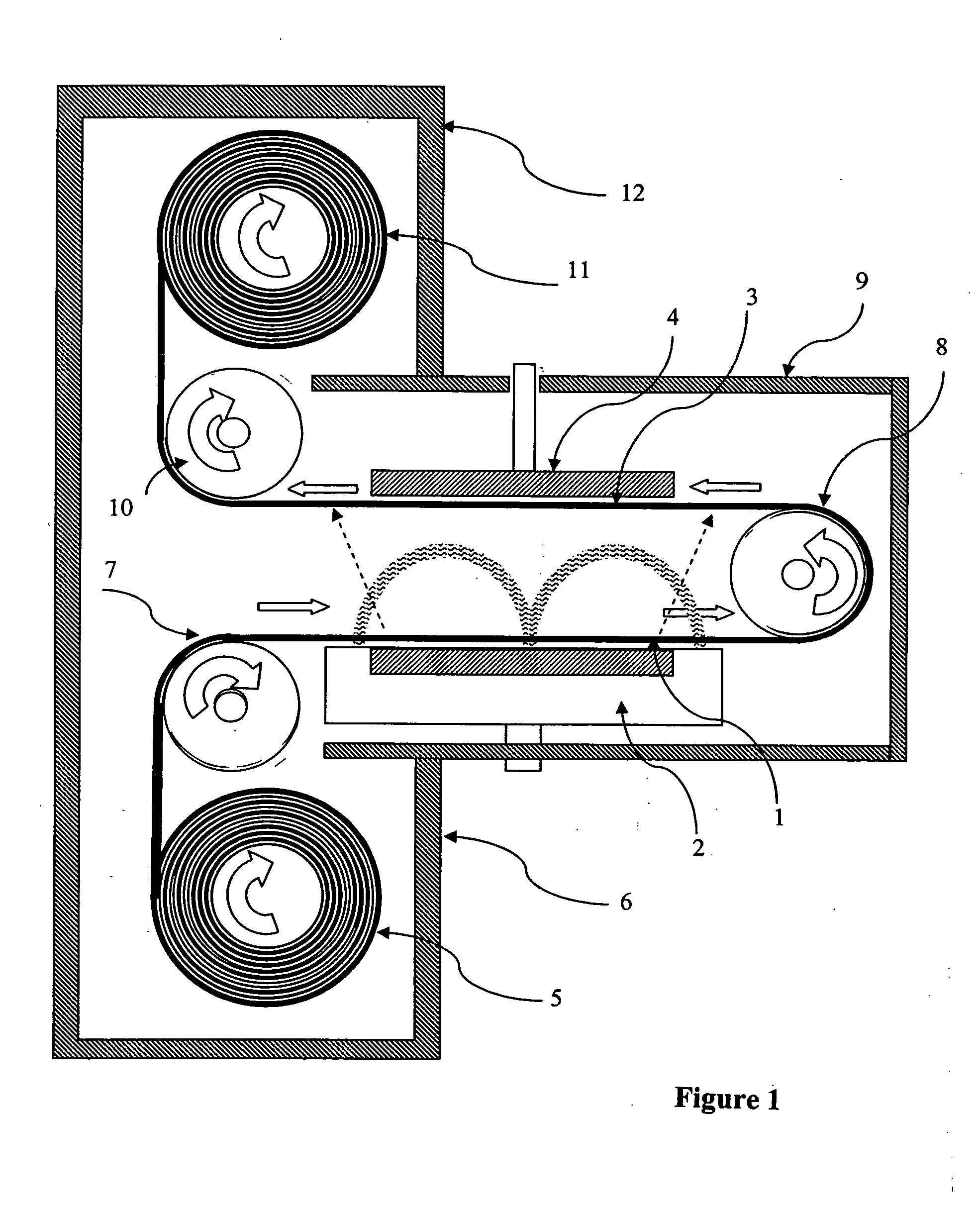
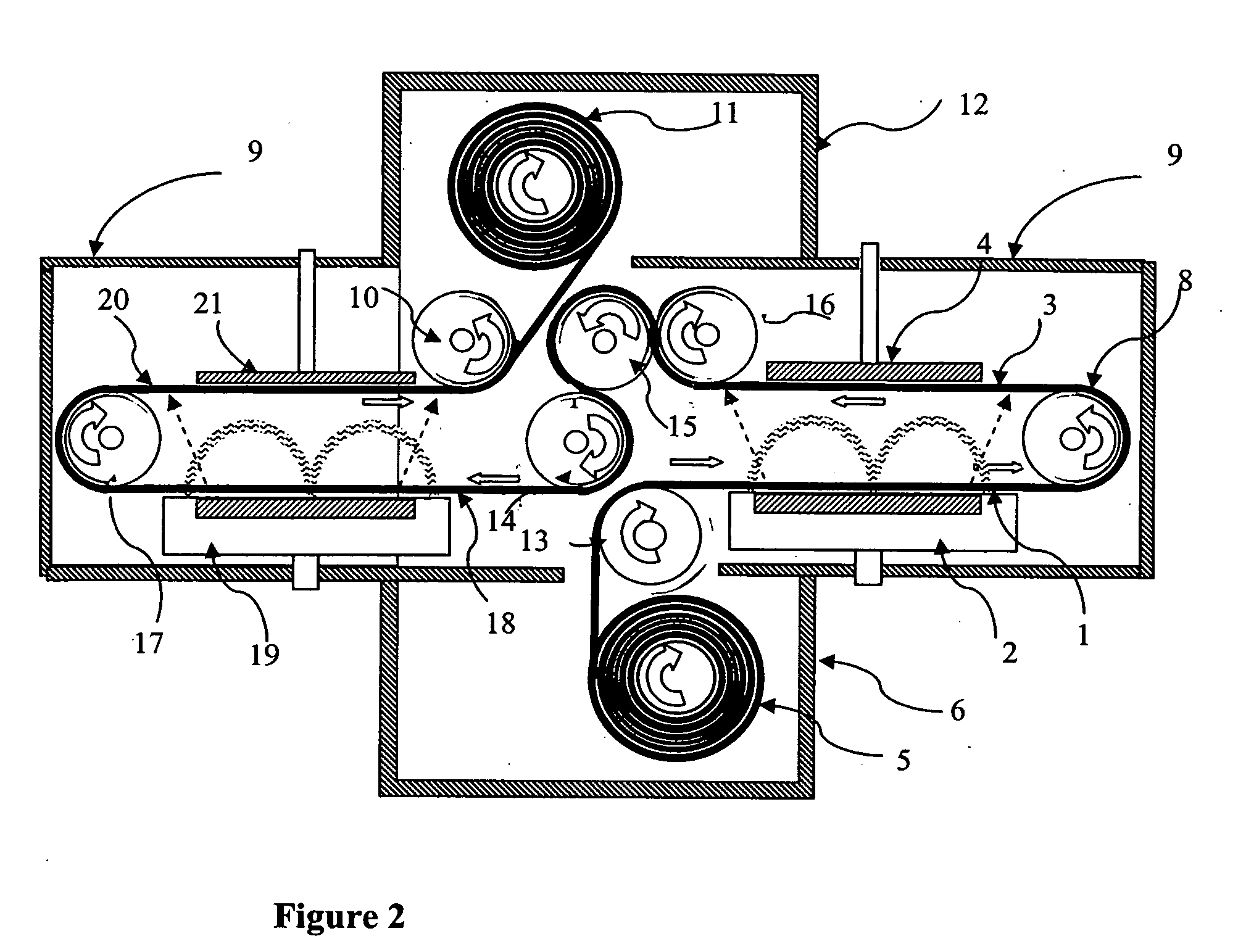
[0129]The deposition time of 10 nm thick film is 0.5 second, the tape speed is 24 m / min. The step-wise procedure is as follows:[0130]1. Two tapes are installed in the chamber in accordance with FIG. 4.[0131]2. The chamber closed.[0132]3. The mechanical pumping line open.[0133]4. Pressure in chamber reached 0.1 ...

example 2

[0148]The copper tapes and polyimide tape are installed in geometry shown on FIG. 4, similarly to the Example 1. The magnetron cathode in the copper branch of the unit is coated with 3 micrometer thick insulating diamond-like coating. The distance between the copper tape and the cathode surface, as well as between polyimide tape and respective cathode surface is 2 mm. The tapes' speed is 8 m / min, sputtering and deposition time for any specific area on the tapes is 1.5 seconds.

[0149]Final thickness of the copper layer upon polyimide is 8 nm. The copper layer is deposited instantly after cleaning of the polyimide substrate by ion sputtering and possesses high adhesion to polyimide and uniformity. Typically in the case of fast moving tape, the variation in uniformity will be less than 0.1% within 1 inch. Uniformity of composition and thickness is much better than plus / minus 1% within 1 m of length.

[0150]With foil, 20-40 microns, and you have a couple of centimeters it's about 10-50 m l...


PUM

PropertyMeasurementUnit
Angleaaaaaaaaaa
Angleaaaaaaaaaa
Angleaaaaaaaaaa

Abstract

A new method of surface engineering of materials employs ion sputtering from a limited area, or sputter zone, of the surface of said materials, and the deposition of the sputtered matter upon a separate or other limited area, or deposition zone, of the surface of the same or simultaneously surface engineered second material, while the sputter and deposition zones are moving synchronously and simultaneously relative to the surface subjected to surface engineering. When the surfaces of two materials are simultaneously engineered, the flux of particles ejected from the sputter zone of the first material are directed to and deposited upon the surface of the deposition zone of the second material, and vice versa; hence, two different materials each possessing both sputter and deposition zones are subjected to surface engineering at the same time resulting in an exchange of surface layers.The new method is named Trans-Zone Sputtering.Where it is applicable, especially in precise surface engineering and ultra-thin film deposition technologies, Trans-Zone Sputtering is characterized by exceptionally high productivity; it does not require expensive consumable targets, and in some instances it avoids the necessity of water cooling, thus simplifying the process and reducing the weight, while simultaneously allowing a thinner magnetron and increasing the effectiveness of the magnetron cathode assembly; it also simplifies the maintenance of the equipment, reduces labor requirements and virtually avoids harmful emissions often occuring with this technology during the equipment maintenance.

Description

BACKGROUND OF THE INVENTION[0001]1. Field of the Invention[0002]The present invention relates to surface nano-engineering using ion sputtering, in particular planar magnetron sputtering, and vacuum deposition of ultra-thin films, typically with thicknesses not exceeding a few hundred angstroms. It especially concerns highly productive surface treatment of materials that may be formed and commercially used as flexible sheets and tapes, including plastics, metals, or composite materials.[0003]2. Description of the Related Art[0004]Over the past few decades, the ion sputtering, especially magnetron sputtering, and in particular, planar magnetron sputtering, revolutionized many industries including microelectronics, data storage, displays, optics, fiber optics, physical instrumentation, telescopes, glass and glazing industry, aerospace and defense applications, automotive industry, decorative coatings, energy technology, lighting, medical applications, and protective coatings.[0005]Magn...

Claims


Application Information

Patent Timeline
IPC IPC(8): C23C14/00
CPCC23C14/022C23C14/3407H01J37/3408H01J37/3277C23C14/562
Inventor DORFMAN, BENJAMIN F.
Owner DORFMAN BENJAMIN F
Features
  • Generate Ideas
  • Intellectual Property
  • Life Sciences
  • Materials
  • Tech Scout
  • Unparalleled Data Quality
  • Higher Quality Content
  • 60% Fewer Hallucinations
Learn More