Method to form a pattern of functional material on a substrate

a functional material and substrate technology, applied in the field of photolithography, can solve the problems of too expensive photolithography, complex multi-step process, limited to forming metal patterns, microcontact printing of devices and components having patterns,

Inactive Publication Date: 2008-02-28
EI DU PONT DE NEMOURS & CO
View PDF20 Cites 92 Cited by
  • Summary
  • Abstract
  • Description
  • Claims
  • Application Information

AI Technical Summary

Benefits of technology

[0011]The present invention provides a method to form a pattern of functional material on a substrate. The method includes providing an elastomeric stamp having a raised surface in a relief structure with a mask material on at least the raised

Problems solved by technology

Photolithography, however, is a complex, multi-step process that is too costly for the printing of plastic electronics.
SAM printing is capable of creating high resolution patterns, but is generally limited to forming metal patterns of gold or silver with thiol chemistry.
However, microcontact printing of devices and components having the pattern of fine resolution lines of functional material separated by relatively large featureless areas where no functional material resides can be problematic.
Sagging of the relief surface can cause the recessed areas to print material where there should be no material.
If the material transferred is large, it may contact one or more

Method used


Image

  • Method to form a pattern of functional material on a substrate
  • Method to form a pattern of functional material on a substrate
  • Method to form a pattern of functional material on a substrate

Examples


example 1

[0067]The following example demonstrates a method to form a pattern on a substrate. Silver nanoparticles are formed into a pattern onto a flexible base that can provide a functional source-drain level of a thin film transistor.

[0068]Master Preparation:

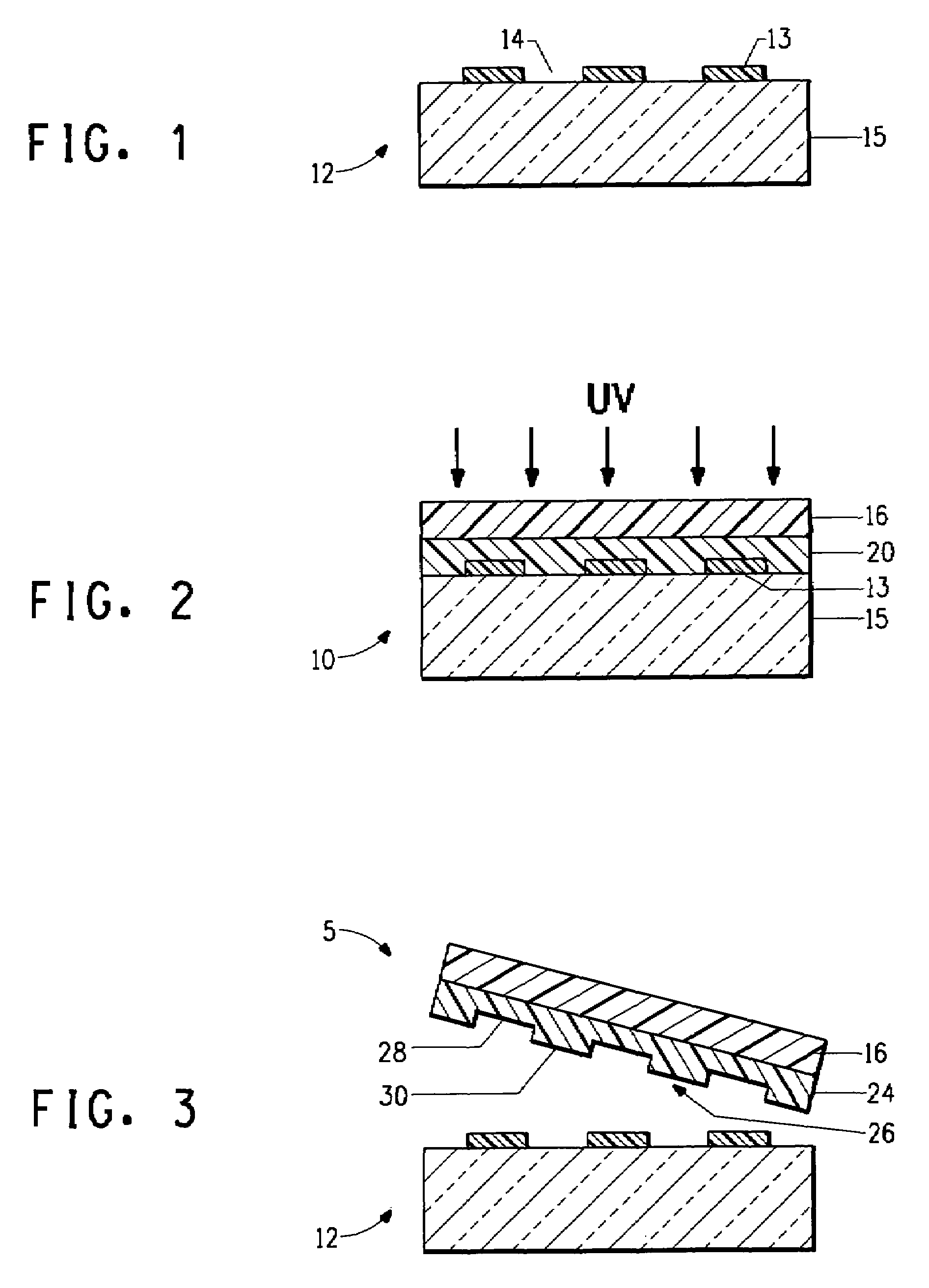
[0069]A thin hexamethyldisilazane layer (HMDS) (from Aldrich) was spun coated onto a 2 inch (5.1 cm) silicon wafer at 3000 rpm for 60 seconds.

[0070]The HMDS is an adhesion promoter for a photoresist material on a silicon wafer. A Shipley positive photoresist, type1811 (from Rohm and Haas) was spun coated onto the HMDS layer at 3000 rpm for 60 seconds. The photoresist film was pre-baked on a hotplate at 115° C. for 1 minute to complete drying. The pre-baked photoresist film was then imagewise exposed through a photomask to ultraviolet radiation of 365 nm for 8 seconds in an I-liner (OAI Mask Aligner, Model 200). After exposure the photoresist was developed in developer type MF-319 (from Rohm and Haas) which is tetramethyl ammonium hydro...

example 2

[0078]The following example demonstrates the method of forming a pattern of functional material using an elastomeric stamp to print a sacrificial mask material. The functional material is silver nanoparticles that form a pattern on a flexible film substrate.

[0079]The master and the elastomeric stamp were prepared as described in Example 1. The relief pattern on the stamp had the same dimensions as those reported for Example 1.

Transfer of Sacrificial Material:

[0080]A sacrificial mask material of a poly(4-vinyl pyridine) (P4VP) solution (from Aldrich, in St Louis, Mo.) was prepared by dissolving the 1% by weight of the P4VP polymer in chloroform (CCl3H) and filtered with 0.2 micron PTFE filter. The P4VP solution was spun coated onto the elastomeric PFPE stamp at 3000 rpm for 60 seconds, and air dried for about 1 minute. The P4VP on the PFPE stamp was then printed onto an acrylic coated side of a 5 mil Melinex® film type ST504 as the substrate, at room temperature without applying any ...

example 3

[0085]The following example demonstrates the method for forming a pattern of a functional material onto a flexible film. The functional material is an organic semiconducting material of a polythiophene.

[0086]The master and the elastomeric stamp were prepared as described in Example 1.

Transfer of Mask Material:

[0087]A solution of 10% by weight of TFE-NB-f-OH copolymer (2-Propanol, 2-[(bicyclo[2.2.1]hept-5-en-2-yloxy)methyl]-1,1,1,3,3,3-hexafluoro-)polymer as shown in the following structure with tetrafluoroethene dissolved in acetone was prepared.

[0088]A mask material of a solution of 1% by weight of Elvacite® 2042, a poly(ethyl methacrylate), (from Lucite) dissolved in acetone was prepared. 10 gr of the TFE-NB-f-OH solution was mixed with 1 gr of the Elvacite solution to form a mixture of a sacrificial masking material. The mask material mixture was spun coated onto the PFPE elastomeric stamp at 5000 rpm for 60 seconds and dried in air. The mask material on the PFPE stamp was contac...


PUM

PropertyMeasurementUnit
Diameteraaaaaaaaaa
Thicknessaaaaaaaaaa
Flexibilityaaaaaaaaaa

Abstract

The invention provides a method to form a pattern of a functional material on a substrate for use in electronic devices and components. The method uses a stamp having a relief structure to transfer a mask material to a substrate and form a pattern of open area on the substrate. The functional material is applied to the substrate in at least the open area. The mask material is removed from the substrate, forming the pattern of functional material on the substrate. The method is suitable for the fabrication of microcircuitry for electronic devices and components.

Description

BACKGROUND OF THE INVENTION[0001]1. Field of the Invention[0002]This invention pertains to a method for forming a pattern of functional material on a substrate, and in particular, the method uses an elastomeric stamp having a relief surface to form a pattern of open area on the substrate where the functional material is applied.[0003]2. Description of Related Art[0004]Nearly all electronic and optical devices require patterning. Microelectronic devices have long been prepared by photolithographic processes to form the necessary patterns. According to this technique a thin film of conducting, insulating, or semiconducting material is deposited on a substrate and a negative or positive photoresist is coated onto the exposed surface of the material. The resist is then irradiated in a predetermined pattern, and irradiated or non-irradiated portions of the resist are washed from the surface to produce a predetermined pattern of resist on the surface. To form a pattern of a conducting met...

Claims


Application Information

Patent Timeline
IPC IPC(8): C23F1/00B29D11/00
CPCB41M2205/14B82Y10/00B82Y40/00G03F7/0002H01L51/0022H05K2203/0537H05K3/048H05K3/1258H05K2201/0257H05K2203/0108H05K3/0079H10K71/611B41M3/00B41F17/00H10K99/00
Inventor BLANCHET, GRACIELA BEATRIZLEE, HEE HYUN
Owner EI DU PONT DE NEMOURS & CO
Why Eureka
Try Eureka