Electro-resistance element, method of manufacturing the same and electro-resistance memory using the same

Inactive Publication Date: 2008-02-28
PANASONIC CORP
View PDF11 Cites 137 Cited by
  • Summary
  • Abstract
  • Description
  • Claims
  • Application Information

AI Technical Summary

Benefits of technology

[0014]According to the present invention, an electro-resistance element that develops less leakage and fewer associated short-circuits even when the electro-resistance layer is made thinner is obtained. Use of such electro-resistance elements enables a highly integrated electro-resistance memory to be obtained.
[0015]Since the

Problems solved by technology

Thus, elements employing an MR effect have a disadvantage that the magnetic field required to reverse the magnetization is enlarged with the miniaturization (densification).
However, when ele

Method used


Image

  • Electro-resistance element, method of manufacturing the same and electro-resistance memory using the same
  • Electro-resistance element, method of manufacturing the same and electro-resistance memory using the same
  • Electro-resistance element, method of manufacturing the same and electro-resistance memory using the same

Examples


example 1

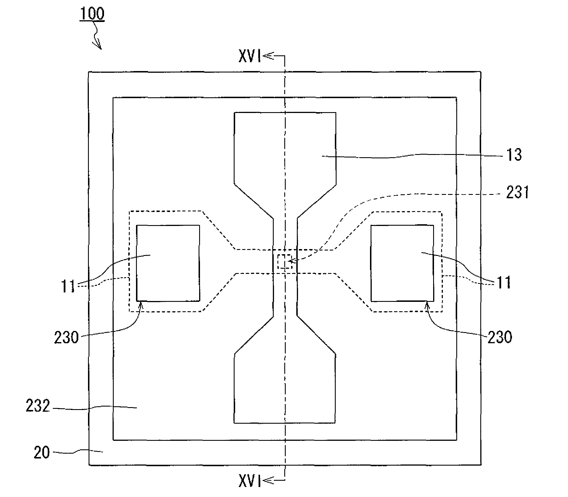
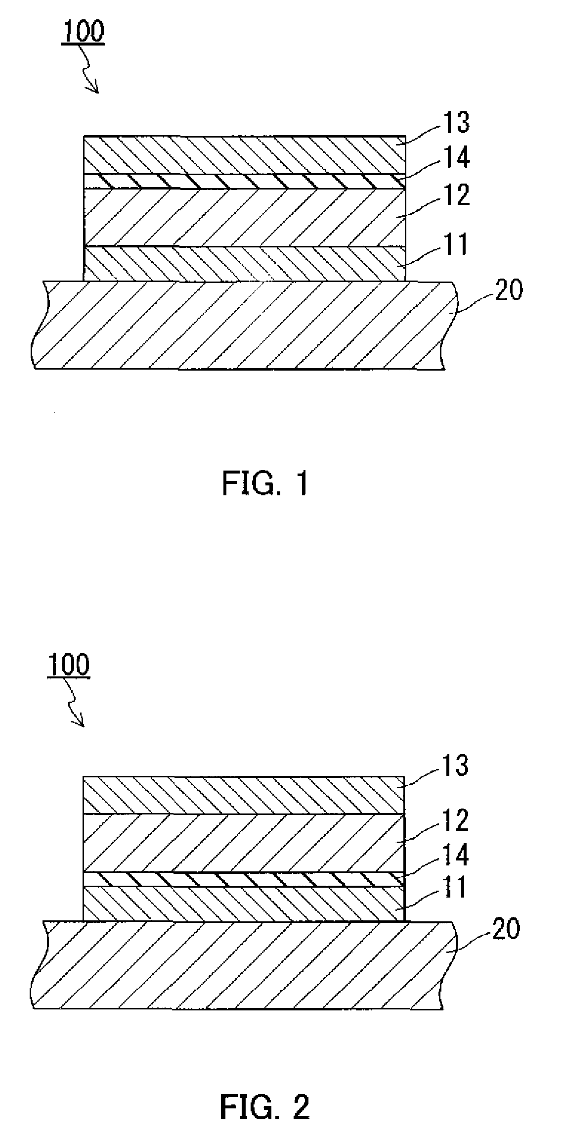
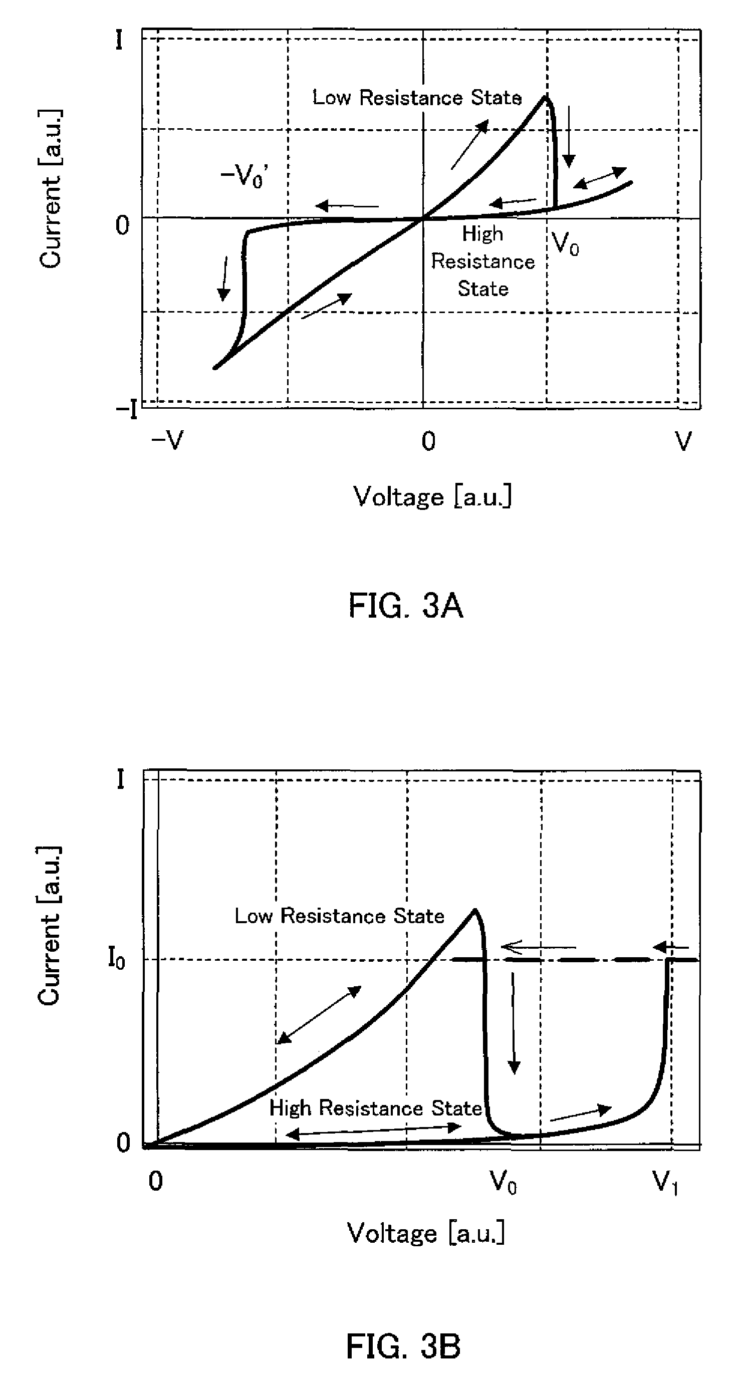
[0127]In Example 1, a sample (an electro-resistance element) including a multilayer structure shown in FIG. 1 and having a form shown in FIG. 15 was fabricated for evaluating its resistance change characteristic. Example 1 employed aluminum oxide (hereinafter, also referred to as “Al—O”) for a material of a tunnel barrier layer 14 and iron oxide (hereinafter, also referred to as “Fe—O”) for a material of an electro-resistance layer 12.

[0128]The sample shown in FIG. 15 was fabricated in the following manner. FIG. 16 shows a cross-sectional view taken along the line XVI-XVI of FIG. 15.

[0129]First, a Si substrate with a thermally oxidized film (a SiO2 film) formed on its surface was prepared as a substrate 20. A lower electrode 11 having a predetermined shape was then formed on the substrate 20 using a metal mask. The lower electrode 11 was formed by stacking a TiAlN layer (200 nm in thickness) and a Pt layer (100 nm in thickness). The TiAlN layer was deposited by magnetron sputtering ...

example 2

[0151]In this Example, a memory element 200 including an electro-resistance element 100 as shown in FIG. 6 was fabricated for evaluating its resistance change characteristic. The tunnel barrier layer 14 employed an aluminum oxide layer (an Al—O layer) and the electro-resistance layer 12 employed an iron oxide layer (an Fe—O layer).

[0152]In the Example 2, the electro-resistance element 100 was formed on a substrate by a known method as shown in FIGS. 13A to 13G. The substrate employed a substrate having a first protective insulating film 103 and a MOS transistor formed thereon. The first protective insulating film 103 employed an ozone TEOS film planarized by CMP (400 nm in thickness).

[0153]A plug 27 formed on the first protective insulating film 103 was composed of a barrier metal 105 made of a titanium film and a titanium nitride film and a plug metal 106 made of tungsten.

[0154]A Ti—Al—N / Pt layer was deposited as a lower electrode layer 11a on that, followed by an Fe—O layer deposi...

example 3

[0165]In the Example 3, a memory element as shown in FIG. 14H was fabricated for evaluating its resistance change characteristic. In this Example, the tunnel barrier layer 14 employed a silicon oxide layer (a Si—O layer) and the electro-resistance layer 12 employed an iron oxide layer (an Fe—O layer).

[0166]In the Example 3, the electro-resistance element 100 and a memory element were formed on a substrate by a known method as shown in FIGS. 14A to 14H. The substrate employed a substrate having a first protective insulating film 103 and a MOS transistor formed thereon. The first protective insulating film 103 employed an ozone TEOS film planarized by CMP (400 nm in thickness).

[0167]First, a lower electrode layer 11a was deposited on the first protective insulating film 103 as shown in FIG. 14A. The hydrogen barrier layer 18 under the lower electrode layer 11a employed a SiN layer (200 nm in thickness). Next, the lower electrode layer 11a was patterned to form a second protective insu...


PUM


Abstract

An electro-resistance element that develops less leakage and fewer associated short-circuits even when an electro-resistance layer is made thinner, a method of manufacturing the same and an electro-resistance memory using the same are provided. The electro-resistance element includes a first electrode, a second electrode, an electro-resistance layer stacked between the first and the second electrodes and an insulating layer (a tunnel barrier layer). The tunnel barrier layer has a thickness in a range from 0.5 nm to 5 nm both inclusive. The electro-resistance layer is a layer having a plurality of states in which electric resistance values are different and being switchable between the states by applying a voltage or a current between the first and the second electrodes. The electro-resistance layer contains transition metal oxide as its main component.

Description

BACKGROUND OF THE INVENTION[0001]1. Field of the Invention[0002]The present invention relates to an electro-resistance element, a method of manufacturing the same and an electro-resistance memory using the same.[0003]2. Related Background Art[0004]In recent years, demands for miniaturization of memory elements have been increasing. Accordingly, electro-resistance memory elements (non-volatile memory elements) that record information by changes in electric resistance, not by changes in charge capacity, have attracted attention as a memory element that is less prone to the adverse effects of miniaturization.[0005]Electro-resistance memory elements include an electro-resistance layer and two electrodes disposed to sandwich the layer. This element can be in a plurality of states in which the electric resistances are different, and the state can be changed by applying a predetermined voltage or current between the electrodes. The one selected state basically is maintained as long as a pr...

Claims


Application Information

Patent Timeline
IPC IPC(8): H01L29/02H01L21/00
CPCG11C13/0007G11C2213/51H01L45/04H01L45/1625H01L45/146H01L27/2436H01L45/12H01L45/1233H10B63/30H10N70/801H10N70/20H10N70/026H10N70/8833H10N70/826
Inventor ODAGAWA, AKIHIRO
Owner PANASONIC CORP
Why Eureka
Try Eureka