AC coupling circuit integrated with receiver with hybrid stable common-mode voltage generation and baseline-wander compensation

a high-speed receiver and ac coupling technology, applied in pulse technique, dc level restoring means or bias distortion correction, baseband system details, etc., can solve the problems of low frequency content errors, baseline wander (blw), and sensitive high-speed data contamination, so as to minimize noise and interference, the effect of minimizing the optimization of circuits

Inactive Publication Date: 2008-03-13
AVAGO TECH WIRELESS IP SINGAPORE PTE
View PDF80 Cites 24 Cited by
  • Summary
  • Abstract
  • Description
  • Claims
  • Application Information

AI Technical Summary

Benefits of technology

[0019]A fully-integrated AC-coupling circuit with hybrid common-mode voltage (Vcm) generation and BLW compensation is proposed. The on-chip generated Vcm eliminates the requirement of an extra chip-pin and additional board-supply for the common-mode voltage, and offers the maximum freedom for circuit optimization. In addition, the heavy penalty resulted from large by-pass capacitors typically required in conventional on-chip Vcm-generation-circuit is avoided. Additional circuitry is included to cancel the BLW by feedback of the recovered data readily available in the receiver. Unlike the previous methods, the proposed circuit mitigates the contamination to the sensitive high-speed data from the high-frequency kick-back noise inherent to the quantized feedback. It also imposes ‘zero’ resistive or capacitive loads to the AC-coupling node. These qualities are of primary co

Problems solved by technology

A receiver of this type is susceptible to noise and fluctuations in the DC and low frequency contents of the signal.
One phenomenon that is a problem in an AC coupled system is baseline wander (BLW), which is signal dependent and varies over time.
BLW affects the low frequency contents of the received signal and can cause errors in the detected data.
The baseline wander is even more severe for an on-chip AC coupled system.
This type of compensator is not practical for multi-Gbps transceivers using current CMOS technology, due to the unrealistic simultaneous requirements of ultra high-speed and high-resolution ADC.
However, the BLW correction interacts and brings difficulty to the DFE adaptation loop.
Both methods are not suitable for high-speed transceivers because of associated cost or interference.
As a result, the ISI can not be linearly passed to the next stage, and is permanently damaged for DFE.
These compensators are not suitable for our application.
However, previous arts in this category are limited to simple circuits, wherein little signal processing is done between the AC coupling corner and the quantization device.
Critical circuit issues such as stable common-mode voltage maintenance, mitigation of high-frequency feed-through from the quantized feedback, and prevention of excess current and capacitive loading from the baseline restoration circuit are not addressed.
When implementing a BLW correction circuit in the signal path before a DFE receiver, a number of design considerations preclude the use of existing methods such as those referred to above.
1) A well defined common-mode voltage is needed before the DFE. The common-mode voltage has fundamental impact on the key pe

Method used


Image

  • AC coupling circuit integrated with receiver with hybrid stable common-mode voltage generation and baseline-wander compensation
  • AC coupling circuit integrated with receiver with hybrid stable common-mode voltage generation and baseline-wander compensation
  • AC coupling circuit integrated with receiver with hybrid stable common-mode voltage generation and baseline-wander compensation

Examples


Embodiment Construction

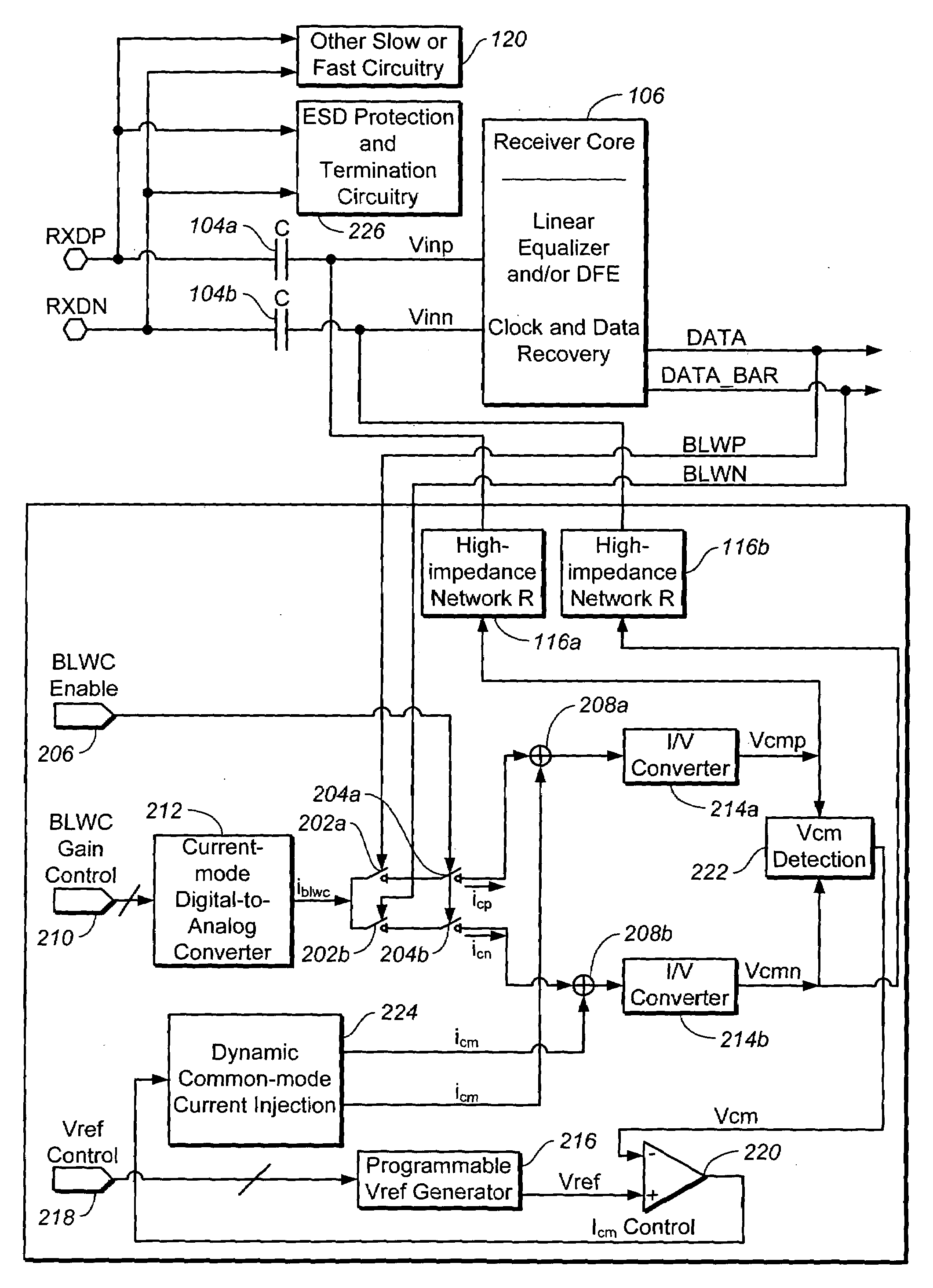
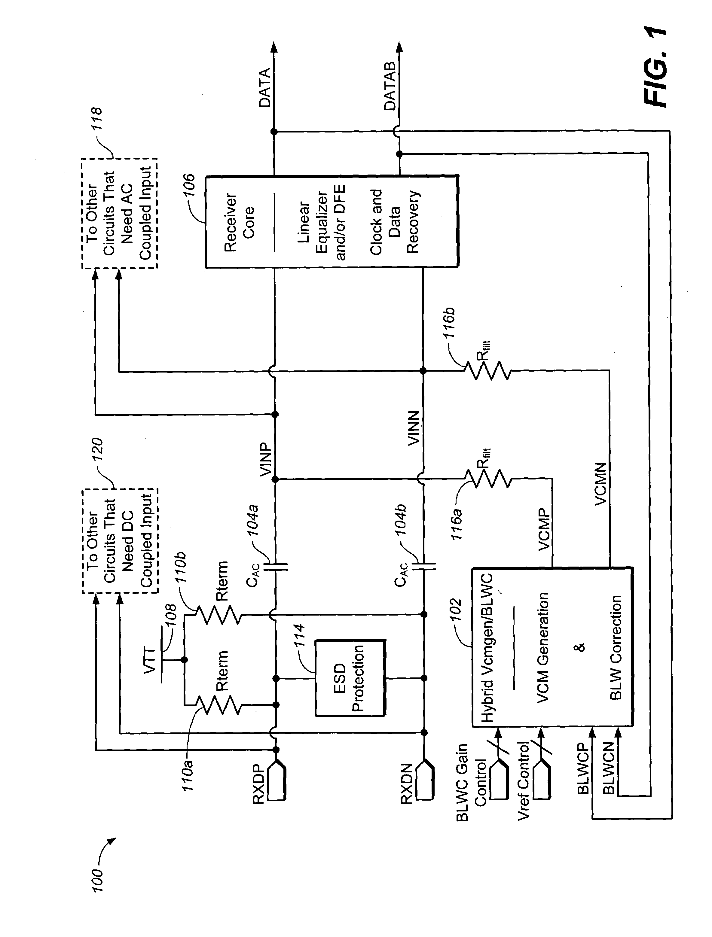
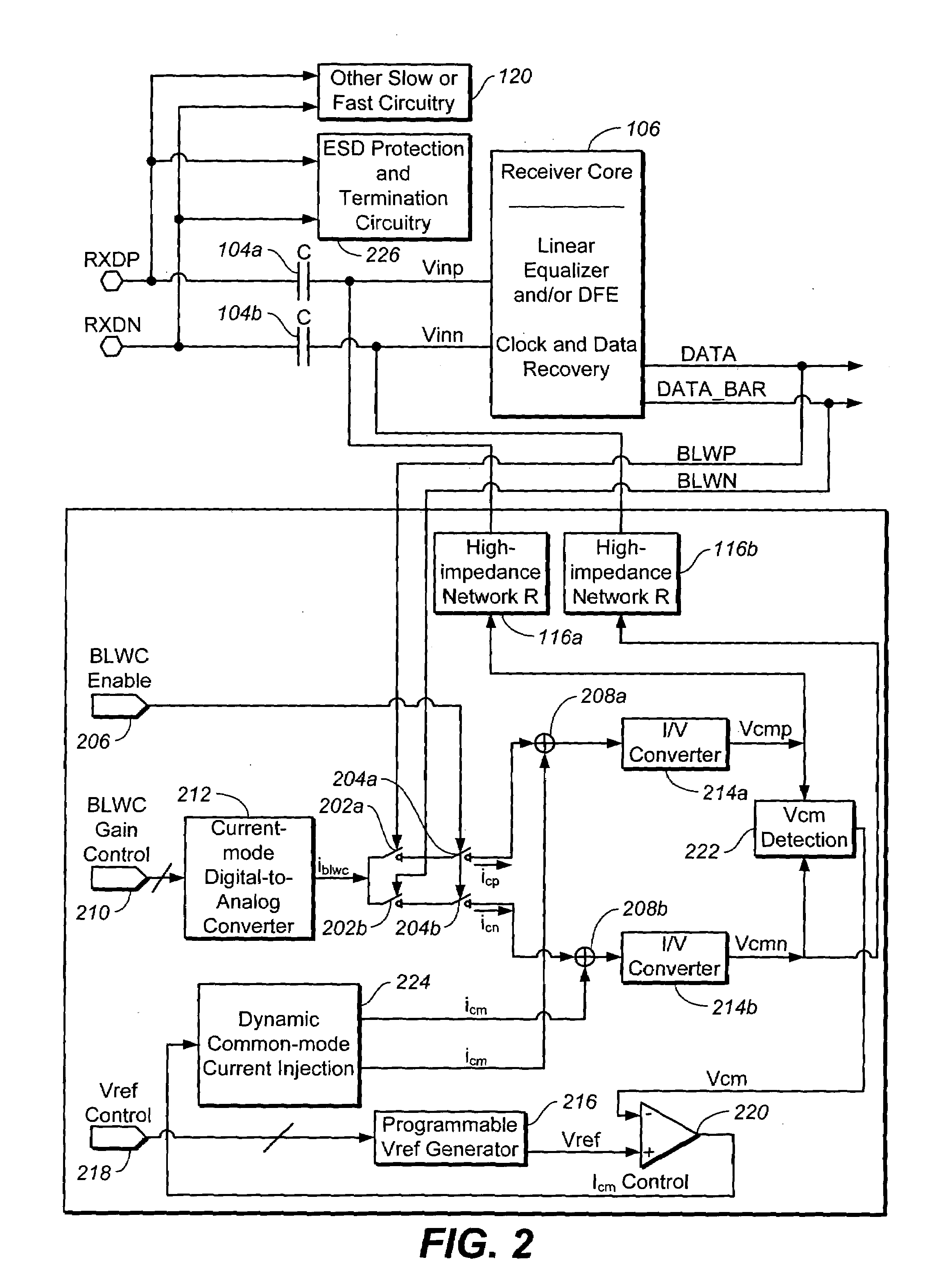
[0026]With reference now to FIG. 1, there is shown a block diagram depicting a receiver 100, provided with a circuit 102 comprising an embodiment of the invention. Receiver 100 usefully comprises the receiver in a high speed backplane transceiver, such as a transceiver operating at 6 Gbps or greater, but the invention is not limited thereto. Moreover, all components of receiver 100 including circuit 102 are usefully integrated together on a single chip or IC. As a further feature, the input signal to the receiver, coupled from the transmitter through a transmission channel, usefully comprises a differential input having positive and negative analog voltage components, RXDP and RXDN, respectively, and a common-mode voltage. The input signal is equal to (RXDP−RXDN), and the common-mode voltage associated with the components is (RXDP+RXDN) / 2.

[0027]Referring further to FIG. 1, there is shown the receiver input signals RXDP / RXDN coupled to an input buffer 106 through capacitors 104a and ...


PUM


Abstract

In a receiver, an AC-coupling solution uses a fully integrated circuit for simultaneously providing both baseline wander compensation and common-mode voltage generation. Usefully, an integrated capacitor is placed between the receiver input pin and the input buffer, and a high resistive impedance element is connected to the internal high-speed data node after the capacitor. An on-chip voltage generation and correction circuit is connected to the other side of the impedance element to generate a common-mode voltage, and to provide dynamic, fine adjustment for the received data voltage level. The voltage correction circuit is controlled by the feedback of data detected by the clock and data recovery unit (CDRU) of the receiver. The feedback data passes through a weighting element, wherein the amount of feedback gain is adjustable to provide a summing weight and thereby achieve a desired BLW compensation. Register bits are used to control an on-chip reference voltage generator that consists of a resistor ladder to generate the reference voltage.

Description

[0001]This application claims the benefit of provisional patent application Ser. No. 60 / 843,305 filed on Sep. 8, 2006, and entitled “Fully Integrated AC Coupling Circuit with Hybrid Stable Common Mode Generation and Zero Load Kick Back Immune Baseline Wander Compensation” which application is hereby incorporated herein by reference.BACKGROUND OF THE INVENTION[0002]1. Technical Field[0003]The present invention relates generally to the field of data transmission and more particularly to circuits for on-chip AC coupling, stable common-mode voltage generation and baseline wander compensation for high-speed receivers. The invention can provide a full suite AC coupling solution including AC coupling, common mode generation, and baseline wander compensation. The solution can be fully integrated, meaning it is all on-chip, does not require any off-chip components, and meets the stringent requirements of preceding a DFE based high-speed transceiver.[0004]2. Description of the Related Art[000...

Claims


Application Information

Patent Timeline
IPC IPC(8): H04L25/00
CPCH04L25/06H04L25/0276
Inventor LIU, CATHY YEZHONG, FREEMAN YINGQUANHSU, SHAO MING
Owner AVAGO TECH WIRELESS IP SINGAPORE PTE
Why Eureka
Try Eureka