Laminated structure, very-large-scale integrated circuit wiring board, and method of formation thereof

a technology of integrated circuit wiring board and laminate structure, which is applied in the direction of liquid/solution decomposition chemical coating, coating, basic electric elements, etc., can solve the problems of poor conductivity, failure of insulation, and inability to reduce the interconnection size of ulsis beyond

Inactive Publication Date: 2008-04-03
WASEDA UNIV
View PDF9 Cites 39 Cited by
  • Summary
  • Abstract
  • Description
  • Claims
  • Application Information

AI Technical Summary

Benefits of technology

[0011]Since the interconnect structure in a ULSI needs a copper wiring layer free of voids and any other defects in its extremely narrow trench, the electroless plating, which is able to be free of voids and the defects, should be carried out in such a way as to prevent peeling from the interlayer insulator.
[0013]a laminated structure includes a low dielectric constant substrate of silicon compound, a barrier layer, and a wiring layer which are firmly bonding to one another, a ULSI interconnect structure based on the laminated structure, and a method for efficiently fabricating them only by wet processes.
[0019]As mentioned above, the monomolecular layer of organosilane compound is modified by a palladium catalyst. The palladium catalyst in a very small amount helps form the NiB layer and the CoWP layer sequentially by electroless plating, and the barrier layer can be efficiently formed on the catalytically activated monomolecular layer only by a wet process. And the resulting barrier layer firmly adheres to the substrate of low dielectric constant material of silicon compound.
[0026]The present invention makes it possible to coat the low dielectric constant material of silicon compound in a simple all-wet process with a firmly adhering barrier layer and an electroless copper plating layer as the wiring layer. the advantage of requiring. Thus, the laminated structure formed in this way includes a substrate of low dielectric constant material of silicon compound, a barrier layer, and a copper layer as the wiring layer formed by electroless plating, which firmly adhere to one another. In addition, the laminated structure is suitable for the copper wiring in a ULSI, particularly the one which is to be formed in a narrower trench than conventional one.

Problems solved by technology

Without this barrier layer, copper that forms the wiring layer diffuses into the interlayer insulator to bring about insulation failure.
The barrier layer of TaN or TiN needs to be coated with a copper seed layer as a conducting layer because it is poor in conductivity, if the wiring layer is to be formed thereon by electric copper plating.
The foregoing method, however, will not reduce the interconnect size of ULSIs beyond the one (equal to or smaller than 100 nm) expected by the industry in near future.
Moreover, the foregoing method needs many steps to fabricate the wiring layer and involves processes differing in phase (dry process for sputtering and CVD and wet process for plating).
Therefore, it is complex and undesirable costwise.
Another disadvantage is that the dry process for sputtering and CVD cannot make a uniform layer as trenches in the wiring layer become narrower than before.

Method used


Image

  • Laminated structure, very-large-scale integrated circuit wiring board, and method of formation thereof
  • Laminated structure, very-large-scale integrated circuit wiring board, and method of formation thereof
  • Laminated structure, very-large-scale integrated circuit wiring board, and method of formation thereof

Examples


example 1

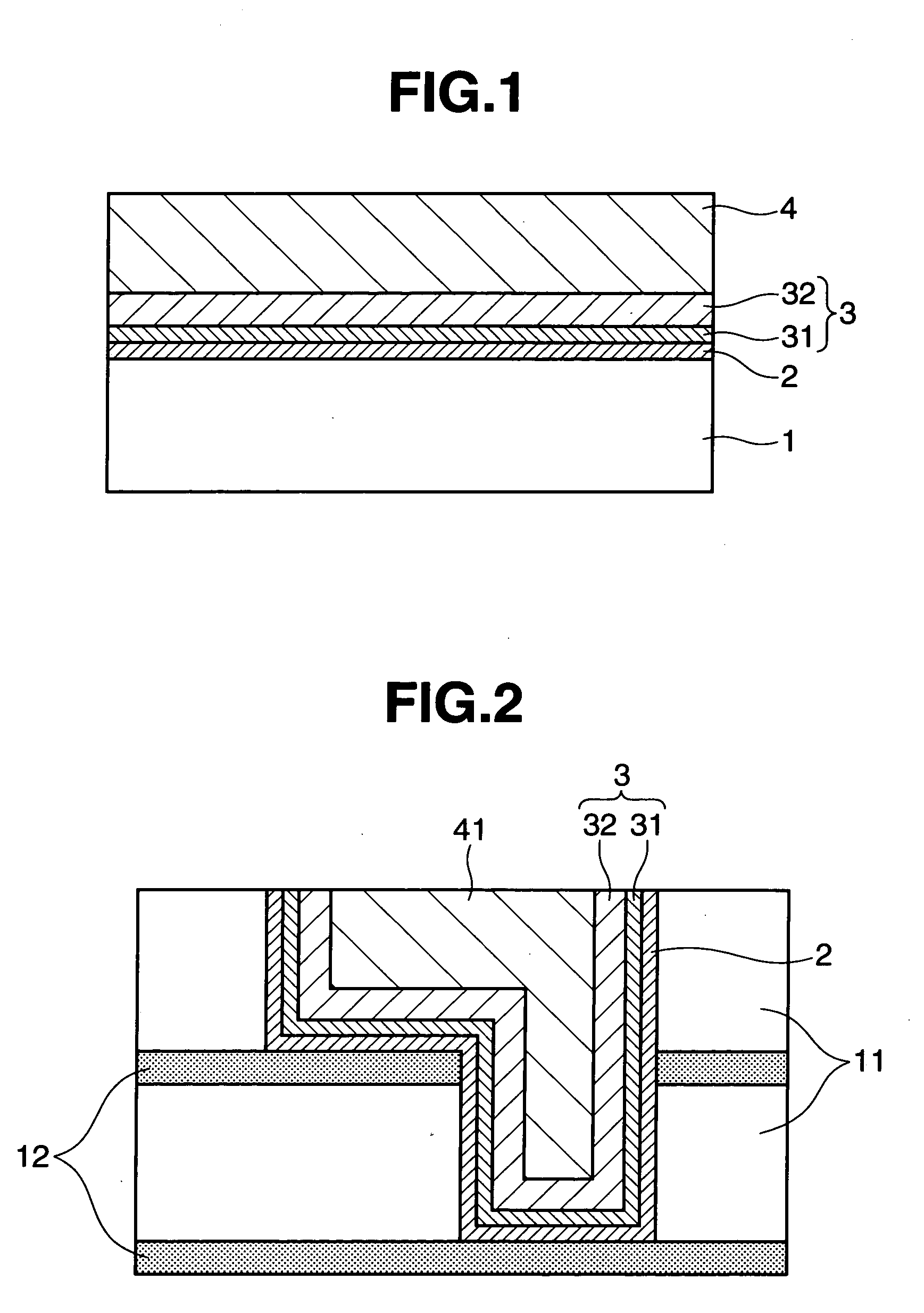
[0075]A silicon substrate (with a 30-nm thick SiO2 coating) was cleaned by SPM treatment [H2SO4:H2O2=4:1 by volume] at 80° C. for 10 minutes. The cleaned silicon substrate was dipped in a solution of N-(2-aminoethyl)-3-aminopropyl-trimethoxysilane in ethanol (1 / 99 by volume) at 50° C. for four hours, for coating with a monomolecular layer of organosilane compound. This step was followed by ultrasonic cleaning in ethanol for removal of excess organosilane compound.

[0076]Next, the silicon substrate was dipped in an aqueous solution specified below at room temperature for ten to 600 seconds so as to modify the monomolecular layer into a catalyst. After this step, the silicon substrate was washed with ultrapure water and then held in ultrapure water.

[0077]

[0078]PdCl2: 0.0005 mol / L

[0079]HCl: 0.016 mol / L

[0080]pH: 1.5 to 2.0

[0081]Subsequently, the silicon substrate was dipped in an NiB electroless plating bath specified below at 70° C. for 30 seconds so that the monomolecular layer of orga...

example 2

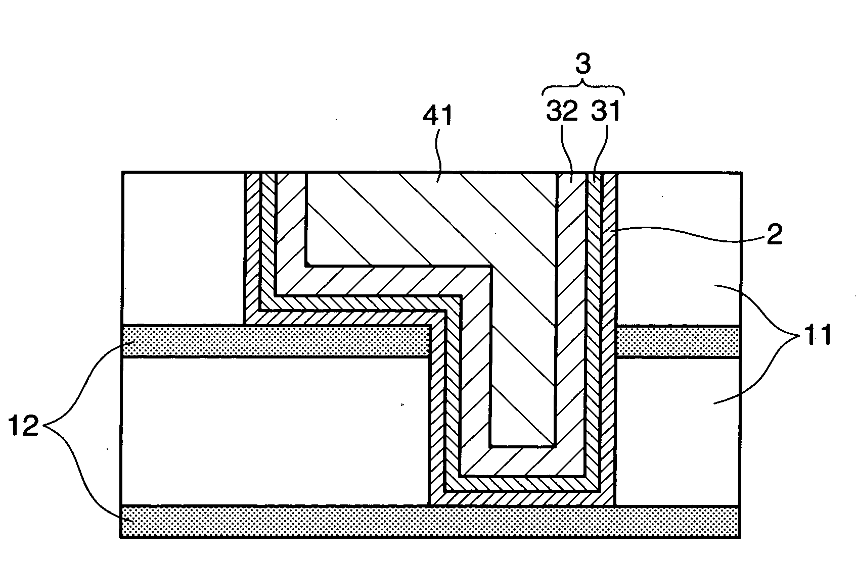
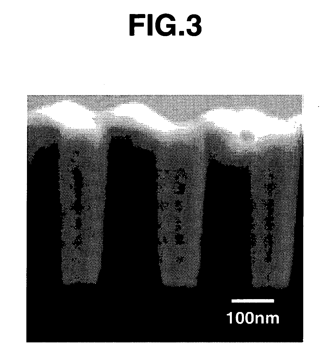
[0132]The same procedure as in Example 1 was repeated to form the monomolecular layer on an SiO2 substrate having a trench pattern formed thereon (100 nm wide, with an aspect ratio (depth / width) of three). The monomolecular layer had its surface modified into a catalyst. Then, the substrate was dipped in an NiB electroless plating bath (as specified in Example 1) at 70° C. for 15 seconds so that the modified monomolecular layer of organosilane compound was coated with an NiB layer (about 10 nm thick). The substrate was dipped again in a CoWP electroless plating bath (as specified in Example 1) at 90° C. for 2 minutes so that the NiB layer was coated with a CoWP layer (about 20 nm thick). The thus formed NiB layer and CoWP constitute the barrier layer.

[0133]The substrate having the barrier layer formed thereon was dipped in a copper electroless plating bath (as specified in Example 1) at 70° C. for 3 minutes so that the barrier layer was coated with a copper layer which fills the tre...


PUM

PropertyMeasurementUnit
widthaaaaaaaaaa
sizeaaaaaaaaaa
temperatureaaaaaaaaaa

Abstract

The laminated structure includes a substrate of low dielectric constant material of silicon compound and an electroless copper plating layer laminated thereon with a barrier layer. The barrier layer is interposed between the substrate and the copper layer, and the barrier layer is formed by electroless plating. And the laminated structure is characterized in that the barrier layer is formed on the substrate with a monomolecular layer of organosilane compound and a palladium catalyst which are interposed between the substrate and the barrier layer, the palladium catalyst modifies the terminal, adjacent to the barrier layer, of the monomolecular layer, and the barrier layer includes an electroless NiB plating layer which is disposed on the substrate side, and a electroless CoWP plating layer.The present invention makes it possible to coat the low dielectric constant material of silicon compound in a simple all-wet process with a firmly adhering barrier layer and an electroless copper plating layer as the wiring layer. the advantage of requiring. Thus, the laminated structure formed in this way includes a substrate of low dielectric constant material of silicon compound, a barrier layer, and a copper layer as the wiring layer formed by electroless plating, which firmly adhere to one another. In addition, the laminated structure is suitable for the copper wiring in a ULSI, particularly the one which is to be formed in a narrower trench than conventional one.

Description

BACKGROUND OF THE INVENTION[0001]1. Field of the Invention[0002]The present invention relates to a laminated structure and a method for its fabrication. The laminated structure is suitable for copper interconnect structure to be formed on a substrate of low dielectric constant material based on a silicon compound. The present invention relates also to a Very-Large-Scale Integrated (ULSI) circuit wiring board and a method for its fabrication. The ULSI circuit wiring board is constructed such that the wiring layer is separated by an interlayer insulator of a low dielectric constant material based on a silicon compound, with a barrier layer interposed between them.[0003]2. Description of the Related Art[0004]The ever-increasing demand for ULSIs with a higher capacity and a lower production cost requires their interconnect structure to have a smaller wiring structure and to be fabricated in a simpler manner. For this reason, the wiring structure in a ULSI is fabricated mainly by the dua...

Claims


Application Information

Patent Timeline
Patent Type & Authority Applications(United States)
IPC IPC(8): H01L23/52
CPCC23C18/1651C23C18/1893H01L2924/0002H01L21/288H01L21/76814H01L21/76826H01L21/76831H01L21/76843H01L21/76846H01L21/76864H01L21/76874H01L23/53238H01L23/53295H01L2924/00
Inventor OSAKA, TETSUYAYOSHINO, MASAHIRO
Owner WASEDA UNIV
Why Eureka
Try Eureka