Method to improve characteristics of pin diode switches, attenuators, and limiters by control of nodal signal voltage amplitude

Inactive Publication Date: 2008-04-17
THE BOEING CO
View PDF2 Cites 8 Cited by
  • Summary
  • Abstract
  • Description
  • Claims
  • Application Information

AI Technical Summary

Benefits of technology

[0017]The present invention provides a method for controlling the local RF impedance in the region of the diodes, using passive RF and microwave impedance transforming techniques. Accordingly, RF voltage amplitude for a given power level may be optimized, resulting in improved operation for all types of PIN diode circuits. Benefits include, a reduction of control voltage amplitude, an increase in power handling capability, reductions in harmonic or inter-modulation distortion, and control of power level threshold in unbiased limiters.
[0018]The impedance at the internal nodes can be varied in most cases, controlling voltage by adjusting the ratio of voltage to current at a given power level. Thus, the same matching techniques can be used to simultaneously control the impedance match at the input and output and the RF/microwave voltage amplitude at internal nodes at the diodes resulting

Problems solved by technology

Increasing voltage amplitude of an RF/microwave signal at higher power levels may cause unwanted changes in 3O the DC condition resulting in undesirable changes in circuit operation.
Re-combination of electrical charge carriers in the intrinsic region of a forward biased diode and the associated rectification effect increase for a large RF signal and can also result in changes.
Changes can also be caused by reverse voltage breakdown.
In addition, high RF voltages can cause significant non-linear changes in parasitic capacitance in the PIN diode under reverse biased conditions.
Voltage driven capacitance changes and resistance changes due to recombination can result in unwanted generation of harmonics and inter-modulation distortion, or mixing effects.
This capacitance, which changes with the instantaneous RF or microwave voltage, results in undesirable generation of harmonic frequencies, or sum and difference inter-modulation frequencies.
Changes in forward current due to re-combination of charge carriers in the intrinsic region also contribute to harmonic distortion and inter-modulation.
In the case of a reverse biased switching diode, the reverse bias DC control voltage must exceed the amplitude of the RF/microwave signal voltage or the diode begins to forward conduct due to the net DC current from the inefficient, yet unavoidable, rectification due to recombination in the intrinsic region.
The DC control voltage cannot be increased without limit because reverse breakdown occurs.
Reverse biased dio

Method used


Image

  • Method to improve characteristics of pin diode switches, attenuators, and limiters by control of nodal signal voltage amplitude
  • Method to improve characteristics of pin diode switches, attenuators, and limiters by control of nodal signal voltage amplitude
  • Method to improve characteristics of pin diode switches, attenuators, and limiters by control of nodal signal voltage amplitude

Examples


Embodiment Construction

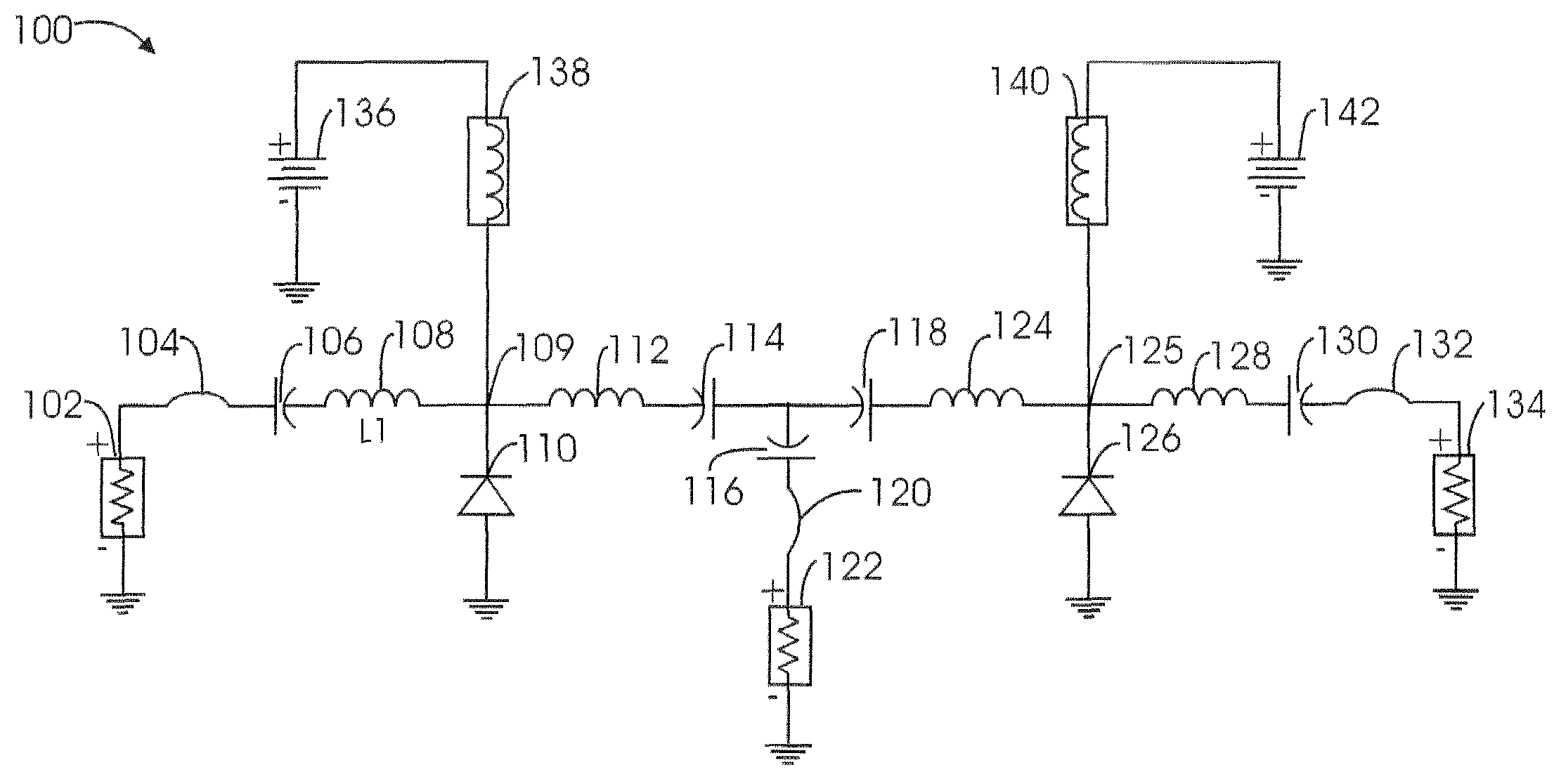
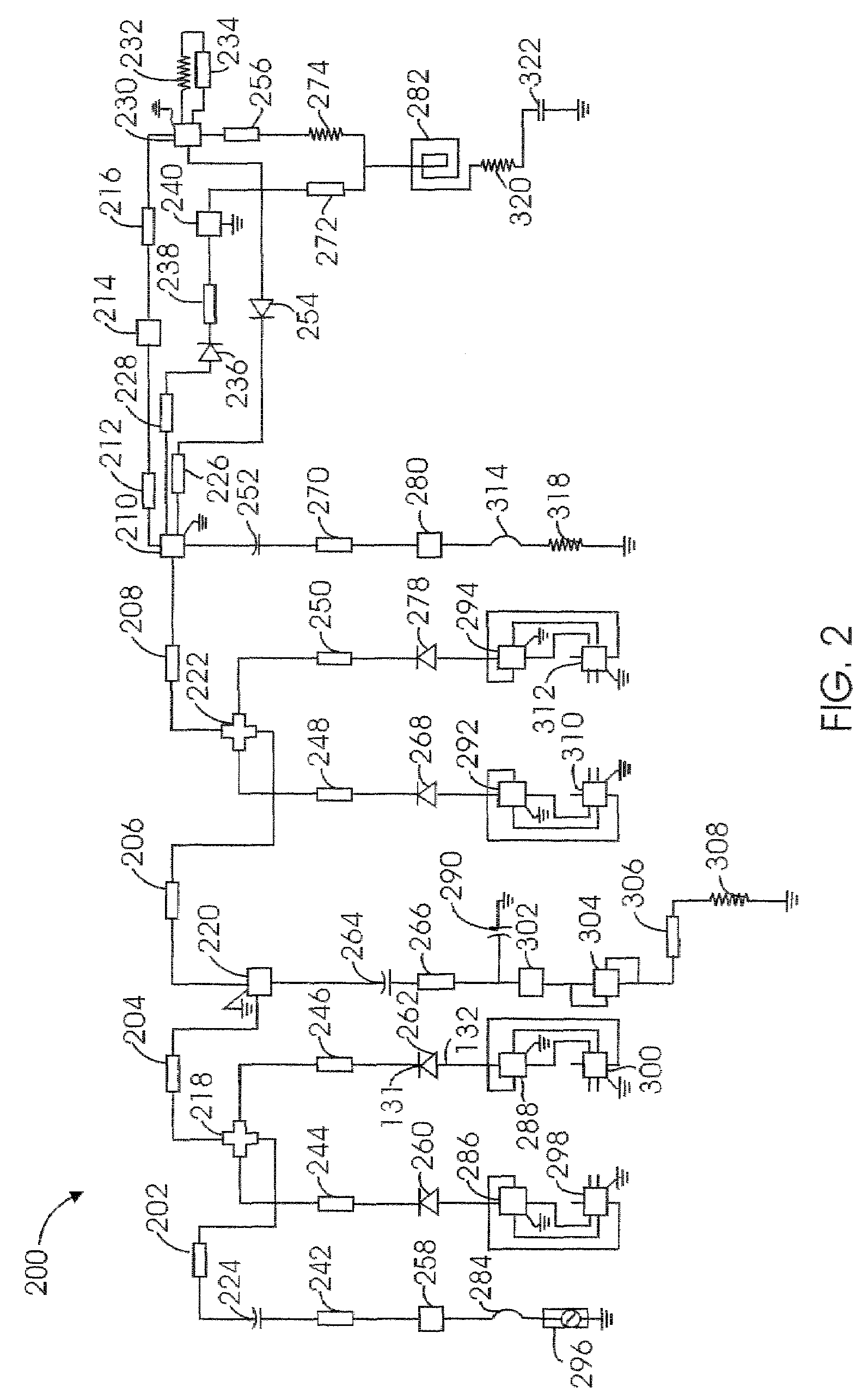
[0027]Although the circuit configurations illustrated in FIG. 1 and FIG. 2 and their associated descriptions employ a Transmit / Receive (T / R) switch, any Radio Frequency (RF) circuit, and microwave circuit that employs PIN diodes as an active element, including attenuators and phase shifters, may be designed with the present invention.

[0028]The present invention provides an iterative technique in which a set of goals are defined and the circuit is modified until the deviation from the goals is minimized. Iterative techniques are used because a mathematical solution in closed form is not available. When continuously variable internal input and output impedances are present between stages, a closed form solution might not exist.

[0029]To better understand and appreciate the invention the operation of a simplified version of a shunt PIN diode antenna T / R switch is discussed below.

[0030]There is a class of switches used in transceiver applications whose function is to connect an antenna t...


PUM


Abstract

A method to improve characteristics of PIN diode switches, attenuators, and limiters via the control of nodal signal voltages by local impedance control.

Description

BACKGROUND[0001]1. Field of the Invention[0002]The present invention is related to RF and microwave circuits, and particularly circuits using PIN diodes designed by minimizing parasitic capacitance of the PIN diode. The method is not limited to circuit designs that minimize or resonate out diode capacitance. Capacitance could even be deliberately introduced and appropriate inductors employed using the method to control impedance at the diode node to advantage.)[0003]2. Related Art[0004]A P-type, Intrinsic, N-type diode (PIN) is a semiconductor device. PIN diodes are constructed with alternating layers of positively doped, intrinsic, and negatively doped semiconductor material. PIN diodes can be used as RF and microwave signal switches, voltage or current controlled attenuators, and limiters. In these applications, the DC bias condition of the diode controls the effective RE or microwave resistance of the diode.[0005]Increasing voltage amplitude of an RF / microwave signal at higher po...

Claims


Application Information

Patent Timeline
IPC IPC(8): H01P1/10H01P5/12
CPCH01P1/185H01P1/15
Inventor KORMANYOS, BRIAN K.
Owner THE BOEING CO
Why Eureka
Try Eureka