
Aligned Carbon Nanotubes And Method For Construction Thereof

a carbon nanotube and aligned technology, applied in the field of aligned carbon nanotubes, can solve the problems of inability to produce defect-free nanotubes, inability to control the growth of cnts in predefined orientations and configurations, and the interface with other materials such as metal electrodes, and conventional cnt production methods lack the ability to form high-aspect-ratio cnt arrays on substrates with uniform height and diameter dimensions. , to achiev

Inactive Publication Date: 2008-04-17
GEORGIA TECH RES CORP
View PDF6 Cites 44 Cited by
  • Summary
  • Abstract
  • Description
  • Claims
  • Application Information

AI Technical Summary

Benefits of technology

[0009]The superior electrical, thermal, and mechanical properties of CNTs promise to bring revolutionary improvement in reducing the interconnect pitch size, increasing thermal conductivity, and enhancing system reliability. Carbon nanotubes are the fascinating one-dimensional molecular structures that can be either metallic or semiconducting, depending on their diameter and helicity. The embodiments of the present invention provide improved CNTs and CNT fabrication methods to solve the above-discussed problems.
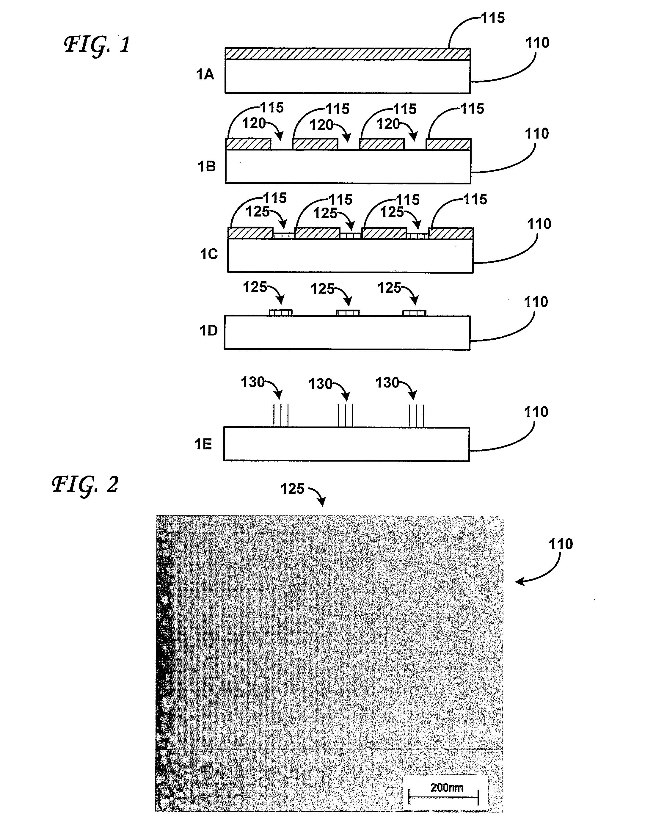
[0010]The remarkable properties of CNTs make them attractive for microelectronic applications, especially for interconnects and nano-scale devices. Some embodiments of the present invention provide a microelectronics compatible process for growing high-aspect-ratio ACNT arrays and CNT films to produce vertical electrical interconnects. Chemical vapor deposition (CVD) can be used to fabricate highly ACNT arrays by introducing ethylene as a carbon source, and argon and hydrogen as carrier gases to an ACNT growth environment according to an embodiment of the present invention. For electronic device applications, CVD methods are particularly attractive due to the characteristic CNT growth features, such as selectivity growth of CNTs where they are required, large area deposition capability, and aligned CNT growth. The CNTs produced in accordance with the various embodiments of the present invention have high purity, and form densely-aligned arrays with controllable array size and height.

Problems solved by technology

As integrated circuit (IC) performance increases, many technical challenges appear in the areas of power delivery, thermal management, input / output (I / O) density, and thermal-mechanical reliability.
For example, conventional manufacturing methods lack the ability to control both the growth of CNTs in predefined orientations and configurations and the interface with other materials such as metal electrodes.
Additionally, conventional CNT production methods lack the ability to form high-aspect-ratio CNT arrays on a substrate with uniform height and diameter dimensions.
Known CNT production methods further lack the ability to produce structurally perfect nanotube growth, produce defect-free nanotubes at macroscopic lengths, and control nanotube growth at specific locations on a substrate or within a device.
Conventional CNTs also have electrical property drawbacks preventing large scale adoption in interconnect applications.
Conventional manufacturing and growth processes lack the ability to produce such high density CNT arrays with high-aspect-ratio nanotubes.

Method used


Image

  • Aligned Carbon Nanotubes And Method For Construction Thereof
  • Aligned Carbon Nanotubes And Method For Construction Thereof
  • Aligned Carbon Nanotubes And Method For Construction Thereof

Examples


Embodiment Construction

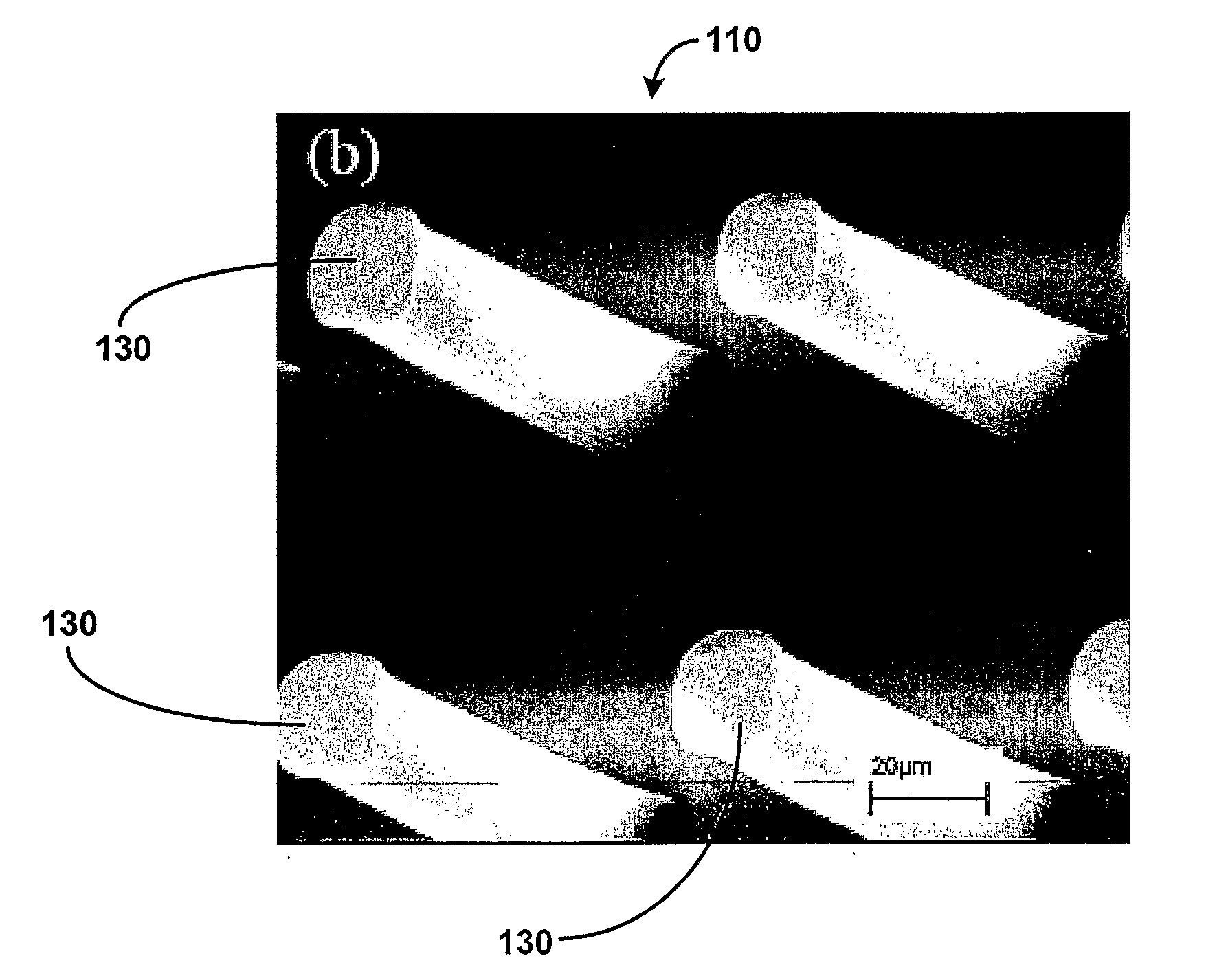
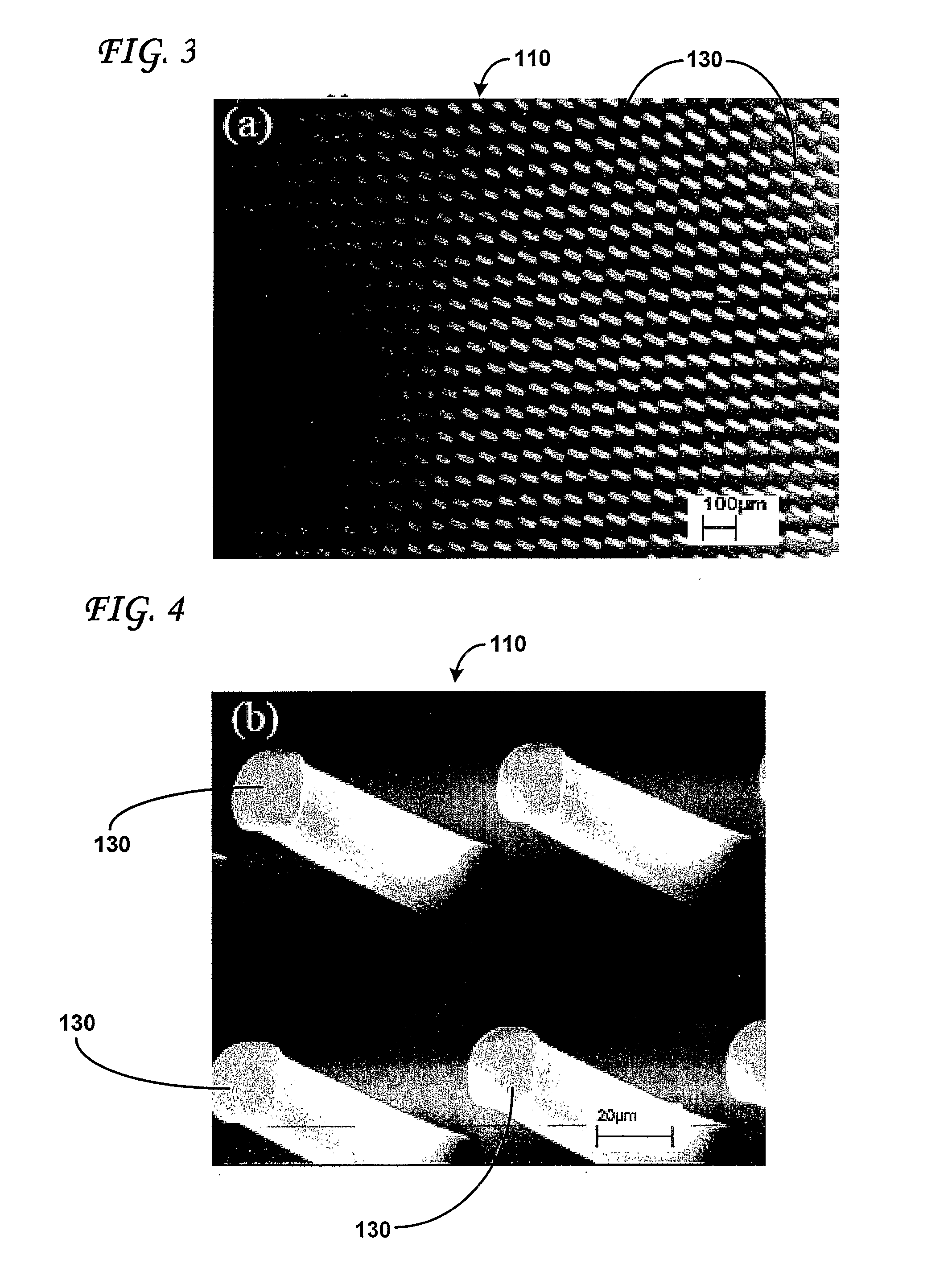
[0031]It should be understood at the outset that an array of carbon nanotubes comprises numerous individual nanotubes, whether the nanotubes are single-walled or have multiple walls. This patent application at times refers to nanotubes individually and collectively (as arrays, bundles, or pillars), however, such reference is not meant to be limiting. Indeed, the discussion of individual nanotubes also applies to an array of nanotubes and vice versa because the production methods and processes discussed herein can be used to create individual nanotubes which form nanotube arrays.

[0032]A preferred embodiment of the present invention provides a simple and efficient method for growing highly-aligned and densely-packed carbon nanotubes under a wide range of growth parameters. For example, at 800° C., ACNTs manufactured in accordance with one embodiment of the present invention grow at an average rate of approximately 100 μm / min. High-resolution transmission electron microscopy HRTEM) cha...


PUM


Abstract

Aligned carbon nanotubes and composites for electrical interconnect and thermal interface materials are provided. In one preferred embodiment, an aligned carbon nanotube device comprises a substrate and a plurality of carbon nanotubes having a substantially vertical profile. The substantially vertical carbon nanotubes are coupled to the substrate. In another preferred embodiment, a carbon nanotube production method comprises depositing a catalyst on a substrate and flowing at least one of argon, hydrogen, and ethylene over the catalyst for a predetermined time at a predetermined temperature to produce a carbon nanotube. This production method enables production of high purity carbon nanotubes and also enables precise placement of carbon nanotubes on a substrate. Other embodiments are also claimed and described.

Description

CROSS-REFERENCE TO RELATED APPLICATIONS[0001]This application claims the benefit of U.S. Provisional Patent Application No. 60 / 621,234, filed 22 Oct. 2004, and U.S. Provisional Patent Application No. 60 / 655,400, filed 23 Feb. 2005, each of which are incorporated herein by reference as is fully set forth below.TECHNICAL FIELD[0002]The present invention relates generally to carbon nanotubes (CNTs), and more particularly, to aligned carbon nanotubes (ACNTs) and methods for constructing ACNTs, which can be utilized in electrical interconnects, thermal interface materials, and nanoscale devices.BACKGROUND[0003]Carbon nanotubes display a well-defined quasi one dimensional cylindrical structure, formed by rolling up graphene sheets of bonded carbon atoms. CNTs can be either metallic or semiconducting, depending on how the graphite layer is wrapped into a cylinder. Metallic CNTs show ballistic conductivity at room temperature. The ballistic conductivity, high thermal conductivity and mechan...

Claims


Application Information

Patent Timeline
IPC IPC(8): G03F7/40C01B31/00
CPCB82Y10/00B82Y30/00B82Y40/00C01B2202/36C01B2202/08C01B2202/26C01B2202/34C01B31/0233C01B32/162
Inventor ZHU, LINGBOWONG, CHING-PONG
Owner GEORGIA TECH RES CORP
Learn More