Si-CONTAINING POLYMERS FOR NANO-PATTERN DEVICE FABRICATION

Inactive Publication Date: 2008-05-01
IBM CORP
View PDF13 Cites 14 Cited by
  • Summary
  • Abstract
  • Description
  • Claims
  • Application Information

AI Technical Summary

Benefits of technology

[0007]The present invention solves the above and other problems by creating a resist polymer that has nano-scale patterns located therein that are in the form of sub lithographic hollow pores (or openings) that are oriented in a direction that is substantially perpendicular with that of its major surfaces (top and bottom). Such a resist polymer having the nano-scale patterns is used as an etch mask for tran

Problems solved by technology

However, use of organic low-k dielectric materials such as, for example, SiLK® (manufactured by Dow Chemical Co., Midland, Mich.) tend to have lower mechanical strength than conventional dielectric materials such as, for example, silicon oxide.
This typically consists of new manufacturing processes and tool sets which add to the overall cost of the fabrication of the semiconductor device.
Also, in sub-resolution lithographic processes, it is necessary to etch wide troughs in empty spaces which, in tur

Method used


Image

  • Si-CONTAINING POLYMERS FOR NANO-PATTERN DEVICE FABRICATION
  • Si-CONTAINING POLYMERS FOR NANO-PATTERN DEVICE FABRICATION
  • Si-CONTAINING POLYMERS FOR NANO-PATTERN DEVICE FABRICATION

Examples


example 1

[0057]Synthesis of a Copolymer of Hydroxystyrene and Methacryl-POSS (90 / 10) (Polymer A)

[0058]10 g of methacryl-POSS, 10.52 g hydroxystyrene and 0.64 g AlBN were dissolved in 40 g THF and charged into a 3-neck flask. The flask was purged with N2 for 30 minutes before the temperature was raised to 62° C. The reaction was carried out overnight under N2. On the next day, the solution was precipitated in 2000 ml of water. The solid thus formed was stirred in 500 ml of hexane, then was filtered off and thereafter washed with hexane. The fine powder polymer was collected and dried in vacuum overnight at 40° C. The molecular weight was determined by GPC to be Mw=12.4 K.

example 2

[0059]Synthesis of a Copolymer of Hydroxystyrene and Methacryl-POSS (95 / 5) (Polymer B)

[0060]7.5 g methacryl-POSS, 22.46 g acetoxystyrene and 1.44 g AlBN were dissolved in 120 g THF and charged into a 3-neck flask. The flask was purged with N2 for 30 minutes before the temperature was raised to 60° C. The reaction was carried overnight under N2. On the second day, the solution was precipitated in 2000 ml of water. The polymer was collected and dried in vacuum overnight at 40° C. The molecular weight was determined by GPC to be Mw=8.05 K.

[0061]One the second day, 26 g of the polymer, 240 ml methanol and 30 ml (30%) ammonia hydroxide were added to the flask and the temperature was kept at 62° C. The reaction was carried out overnight in N2. On the third day, the solution remained blur. The solution was rotary evaporated dried to form a solid. The solid thus formed was washed with water, and then mixed in 200 ml THF, 100 ml methanol, and 20 ml of ammonium hydroxide. After overnight unde...

example 3

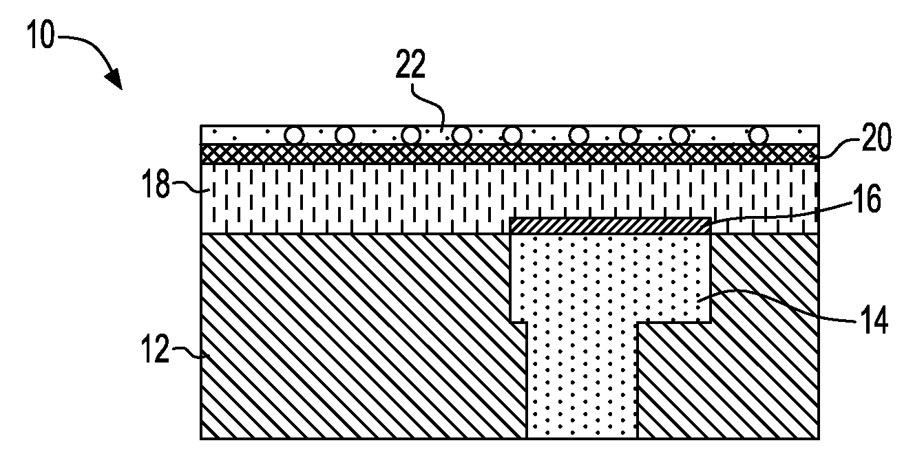
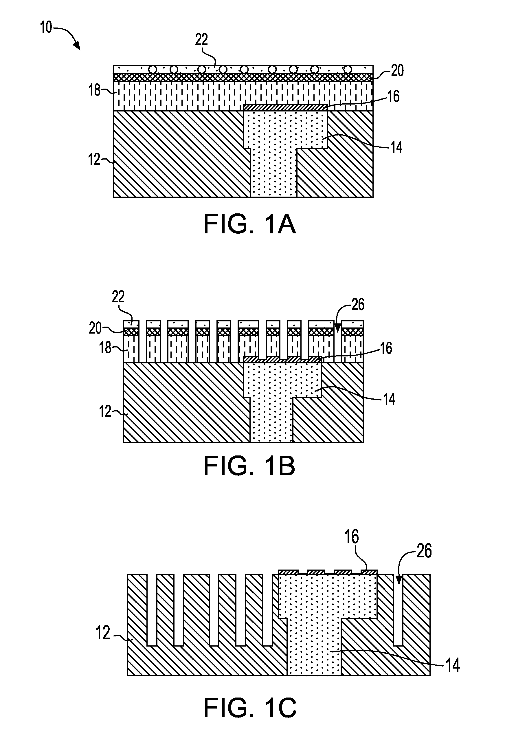
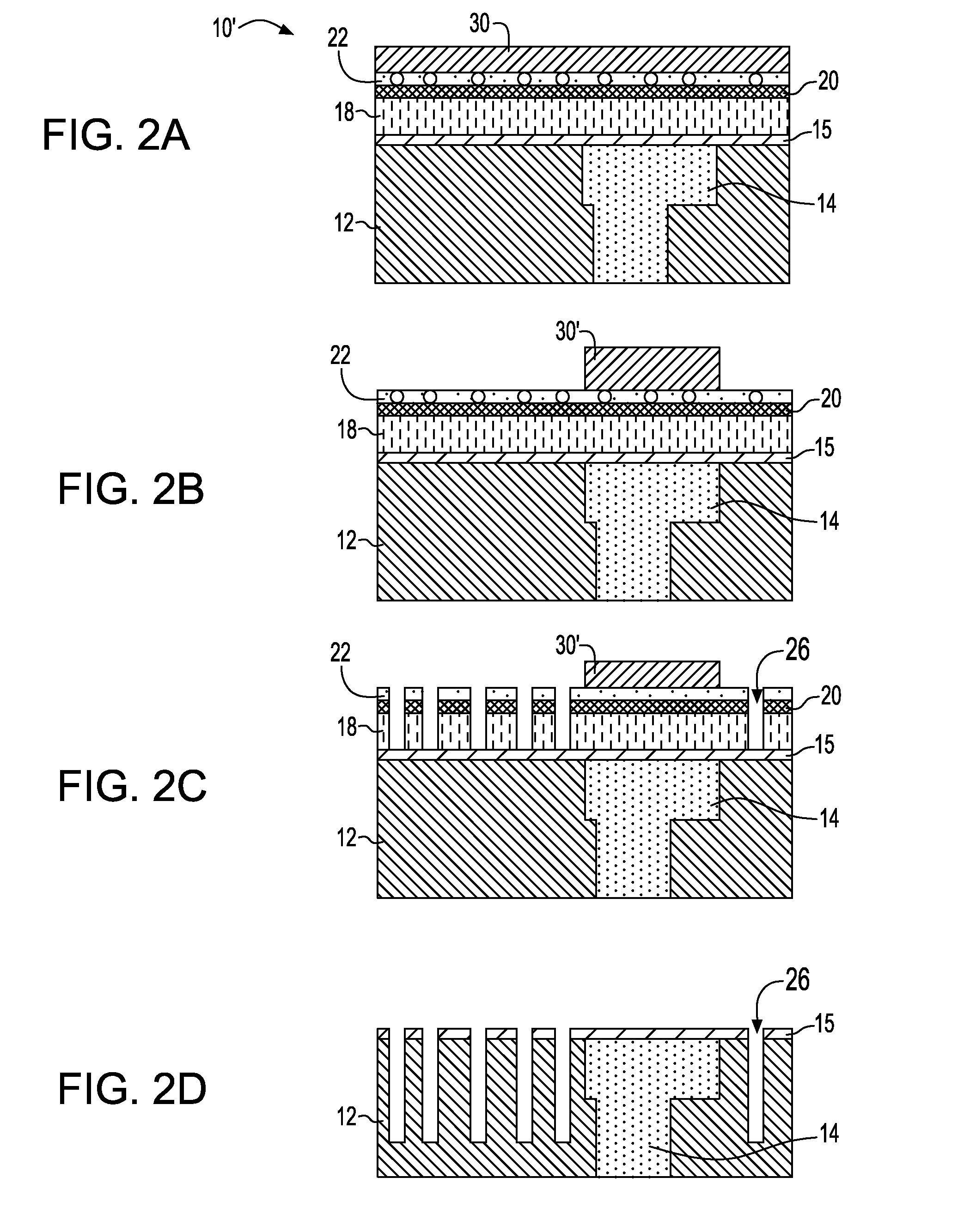
[0062]Creation of Nano-Scale Patterns with Circular Top Openings on the Polymers

[0063]Polymer A from Example 1 was dissolved in cyclohexanone to form 1.14 wt % and 0.5 wt % polymer solutions. Both solutions were spin coated on Si wafers using a spin speed of 1500 rpm, and then baked on hot plate at 110° C. for 90 sec to give thicknesses of about 35 nm and 20 nm, respectively. Both wafers were subjected to a reactive ion etching process using CF4 as an etchant. The top down SEM images of etched wafers exhibited many circular holes with diameter around 20 nm. The 20 nm thick film exhibited higher density of holes than the 35 nm thick one. The same experiment was carried out on Polymer B obtained from Example 2 with 1 wt % and 0.5 wt % polymer solutions. The results of creating circular holes were very similar to those obtained on Polymer A.


PUM


Abstract

A resist polymer that has nano-scale patterns located therein that are in the form of sub lithographic hollow pores (or openings) that are oriented in a direction that is substantially perpendicular with that of its major surfaces (top and bottom) is provided. Such a resist polymer having the nano-scale patterns is used as an etch mask transferring nano-scale patterns to an underlying substrate such as, for example, dielectric material. After the transferring of the nano-scale patterns into the substrate, nano-scale voids (or openings) having a width of less than 50 nm are created in the substrate. The presence of the nano-scale voids in a dielectric material lowers the dielectric constant, k, of the original dielectric material. In accordance with an aspect of the present invention, the inventive resist polymer comprises a copolymer that includes a first monomer unit (A) that contains a Si-containing component, and a second monomer unit (B) that contains an organic component, wherein said two monomer units (A and B) have different etch rates.

Description

FIELD OF THE INVENTION[0001]The present invention relates to semiconductor device manufacturing, and more particularly to a method for manufacturing sub lithographic openings in a Si-containing material, which material is then subsequently used as an etch mask for transferring the sub lithographic openings to an underlying dielectric material. The presence of the sub lithographic openings in the dielectric material lowers the overall dielectric constant of the dielectric material.BACKGROUND OF THE INVENTION[0002]To fabricate microelectronic semiconductor devices such as an integrated circuit (IC), many different layers of metal and insulation are selectively deposited on a semiconductor. The insulation layers may be, for example, silicon dioxide, silicon oxynitride, fluorinated silicate glass (FSG) and the like. These insulation layers are deposited between the metal layers, i.e., interlevel dielectric (ILD) layers, and may act as electrical insulation therebetween or serve other kn...

Claims


Application Information

Patent Timeline
IPC IPC(8): G03C1/00
CPCG03F7/0758G03F7/0045
Inventor CHEN, KUANG-JUNGHUANG, WU-SONGLI, WAI-KINLIN, YI-HSIUNG S.
Owner IBM CORP
Why Eureka
Try Eureka