Organic light emitting display and fabrication method thereof

a technology of light-emitting display and organic material, which is applied in the manufacture of electrode systems, electric discharge tubes/lamps, discharge tubes luminescnet screens, etc., can solve the problems of not fully developed, difficult to fabricate an oled having a thickness less than 1 mm, and protect film technology, which can replace the contemporary sealing technology, etc., to achieve the effect of small thickness

Inactive Publication Date: 2008-05-15
SAMSUNG DISPLAY CO LTD
View PDF46 Cites 21 Cited by
  • Summary
  • Abstract
  • Description
  • Claims
  • Application Information

AI Technical Summary

Benefits of technology

[0013]Another object of the present invention is to provide a fabrication method of an organic light emitting display that prevents bending and damages of a substrate of the organic light emitting display during the fabricating processes.
[0014]Another object of the present invention is to reduce process time for fabrication of an organic light emitting display, and thereby to improve productivity and to reduce cost for fabrication of an organic light emitting display.

Problems solved by technology

A protection film technology, which can replace the contemporary sealing technology, however, is not yet completely developed, and thus it is difficult to fabricate an OLED having the thickness small than 1 mm.
In these methods described above, however, there exists a problem that the process time for the fabrication becomes extremely long, because an etching or grinding process has to follow the process for forming a semiconductor layer or an organic light emitting diode, and the process for laminating the substrates.
Moreover, there is high possibility that a glass substrate, a semiconductor layer, and an organic light emitting diode can be damaged or destroyed during the lamination process, and thus there are problems that the production yield is low and the fabrication cost becomes high.
In this case, however, the glass substrate is so thin that the glass substrate is easily bent during transportation of the substrate from one process to the other process, or is easily damaged when the substrate is mechanically shocked during the transportation.

Method used


Image

  • Organic light emitting display and fabrication method thereof
  • Organic light emitting display and fabrication method thereof
  • Organic light emitting display and fabrication method thereof

Examples


Embodiment Construction

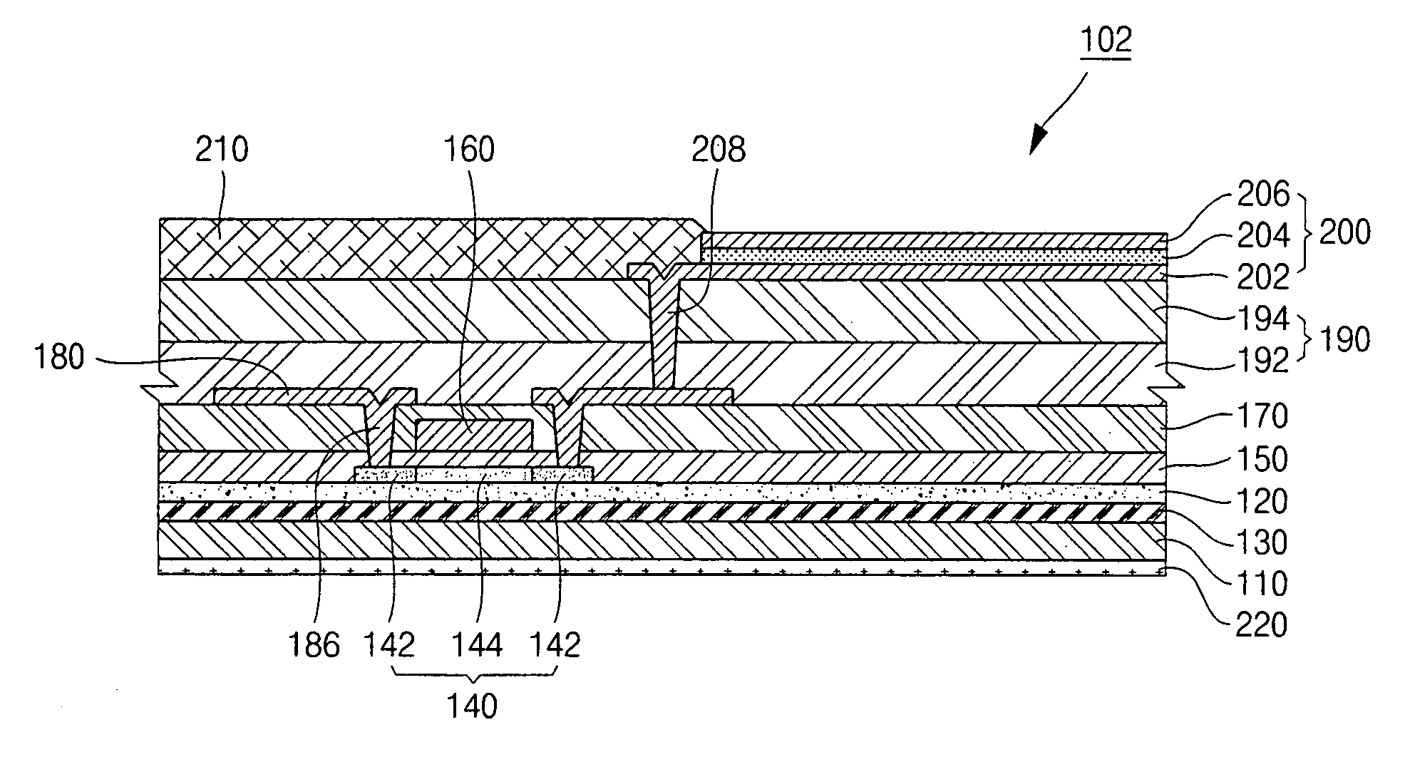
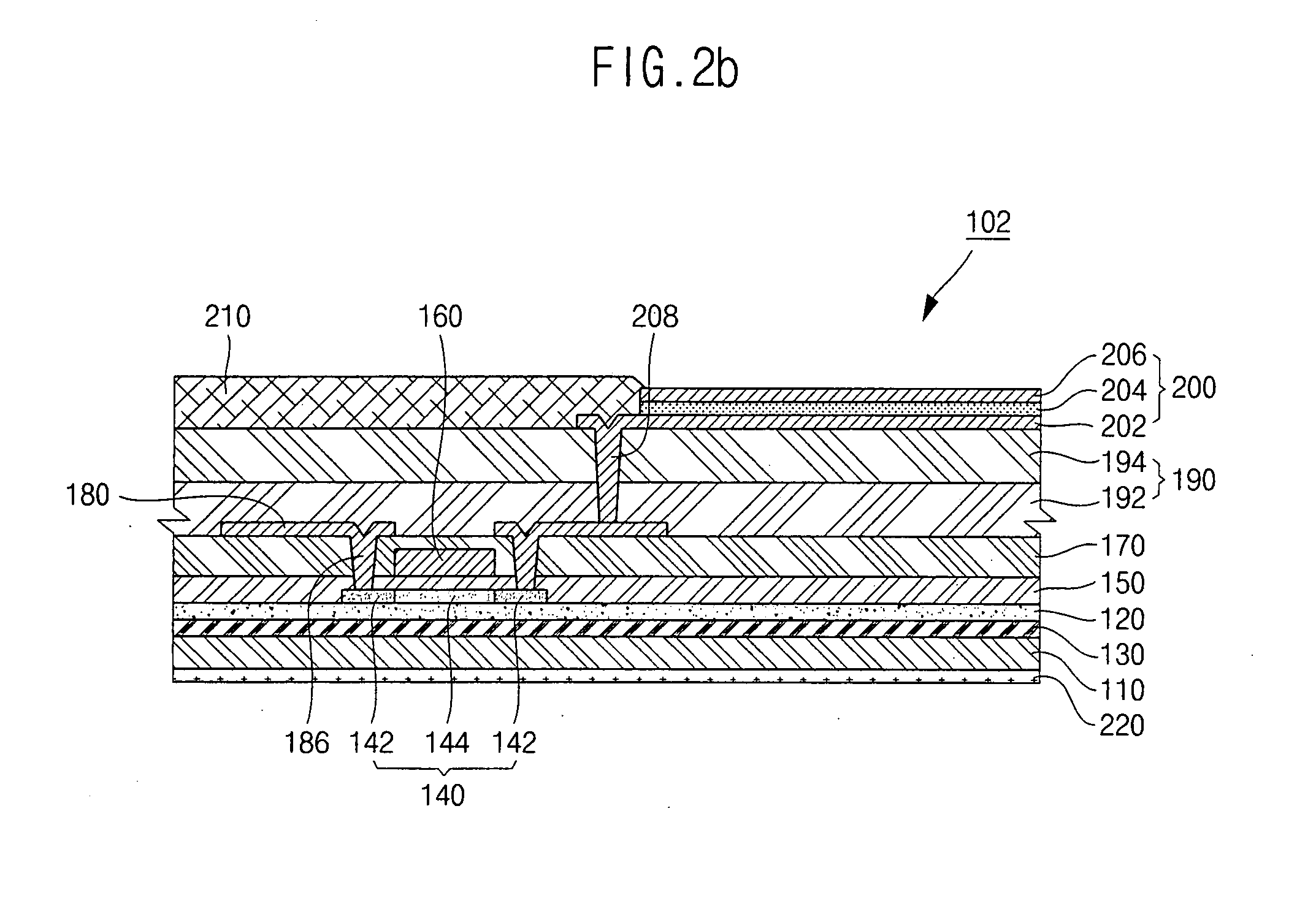
[0030]The preferred embodiment of the present invention will be explained in detail with referring to the attached drawings so that the present invention can be derived by the person having ordinary skills in the field to which the present invention belongs.

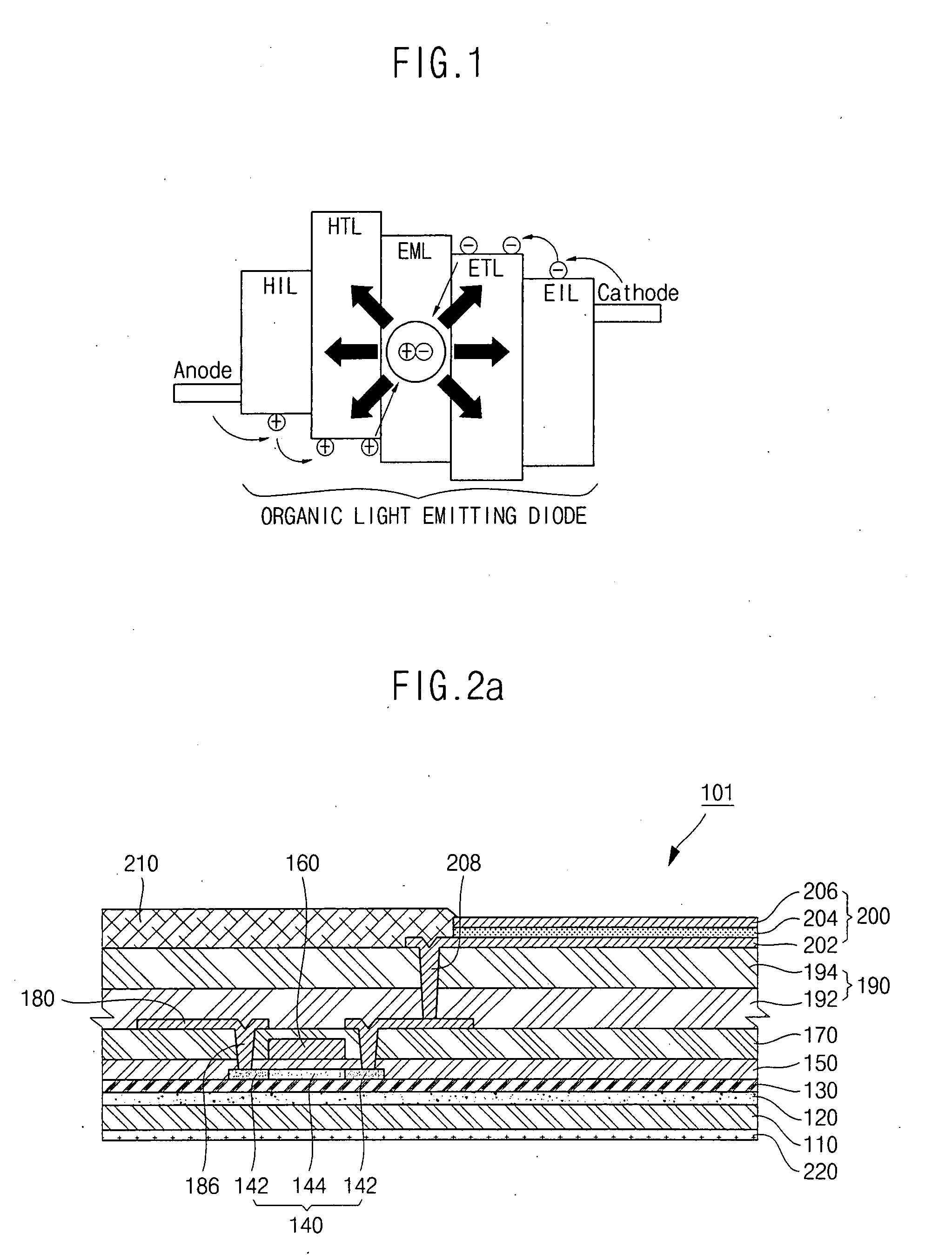
[0031]FIG. 1 shows a schematic diagram of an organic light emitting diode. As illustrated in FIG. 1, an organic light emitting diode includes an anode, a cathode, and an organic layer disposed between the anode and the cathode. The organic layer can include an emission layer (EML) which emits light when electrons and holes are recombined and thereby an exciton is formed, an electron transport layer (ETL) that transports electrons, and a hole transport layer (HTL) that transports holes. Furthermore, in the electron transport layer (ETL), an electron injection layer (EIL) for improving effectiveness of the electron injection can be further formed. In the hole transport layer, a hole injection layer (HIL) for improving effectiveness...


PUM


Abstract

An organic light emitting display having a small thickness and a fabrication method thereof are provided. The organic light emitting display includes a substrate, an non-transmissive layer formed on the substrate, a semiconductor layer formed on the non-transmissive layer, a gate insulation layer formed on the semiconductor layer, a gate electrode formed on the gate insulation layer, an inter-layer dielectric layer formed on the gate electrode, a source / drain electrode formed on the inter-layer dielectric layer, an insulation layer formed on the source / drain electrode, and an organic light emitting diode formed on the insulation layer.

Description

CLAIM OF PRIORITY[0001]This application makes reference to, incorporates the same herein, and claims all benefits accruing under 35 U.S.C. §119 from an application for ORGANIC LIGHT EMITTING DISPLAY DEVICE AND MANUFACTURING METHOD THEREOF AND MOVING DEVICE THEREFOR earlier filed in the Korean Intellectual Property Office on 10 Nov. 2006 and there duly assigned Serial No. 10-2006-0111300.BACKGROUND OF THE INVENTION[0002]1. Field of the Invention[0003]The present invention relates to an organic light emitting display and a fabrication method thereof, and in particularly, relates to an organic light emitting display and a fabrication method thereof, in which an organic light emitting display has a small thickness, an organic light emitting layer and semiconductor layers are protected from UV-ray during or after fabrication processes of the organic light emitting diode, damages of the substrate of the organic light emitting diode during the fabrication processes are prevented, and the f...

Claims


Application Information

Patent Timeline
Patent Type & Authority Applications(United States)
IPC IPC(8): H05B33/00H01L51/50
CPCH01L27/3272H01L2251/566H01L51/56H10K59/126H10K71/851H10K71/00H05B33/22H05B33/10
Inventor KIM, JONG-YUNCHOI, BYOUNG-DEOG
Owner SAMSUNG DISPLAY CO LTD
Why Eureka
Try Eureka