RF resonator system and method for tuning an RF resonator system

a resonator and frequency technology, applied in the field of radiofrequency resonator system, can solve the problems of lithography, difficult to interrupt conductors without damaging adjacent conductors, and the greatest voltage difference between adjacent conductors at the end of finger capacitors, so as to reduce the perturbation of static magnetic field, reduce the perturbation of the static magnetic field, and avoid large step changes in the dielectric constant

Active Publication Date: 2008-05-15
BRUKER SWITZERLAND AG
View PDF10 Cites 17 Cited by
  • Summary
  • Abstract
  • Description
  • Claims
  • Application Information

AI Technical Summary

Benefits of technology

[0037]Setting the required resonance frequency is performed by choosing the thickness of the dielectric layers. In principle, it is enough to cover at least one region at which a high electrical field prevails with a dielectric layer. To additionally protect the resonator system against breakdowns, it is advantageous to coat all regions in which the electric fields are strongest to distribute the electric fields as homogeneously as possible over the space and avoid large step changes in the dielectric constant, especially, at spikes and edges. The dielectric layer can be applied with varying thicknesses to different points of the resonator so that the local thicknesses of the layer vary over the surface of the resonator. To achieve the most homogeneous possible current distribution as well, it is advantageous if the surface of the resonator to which the conductive structures are applied is completely covered by the dielectric layer or layers. Coverage should then be largely even over the surface of the resonator system, i.e. the thickness variation should be under 10%, if possible. For such resonator systems, the distribution of the current density in the conductor elements is especially simple to calculate and adapt and the adaptation is independent of the set resonance frequency, i.e. trimming. Furthermore the constant coverage with a dielectric layer reduces the perturbation of the static magnetic field if the inventive resonator system is to be used in a magnetic resonance probe.
[0038]In an advantageous variant of the inventive method, after application of the first dielectric layer, a further dielectric layer is applied to the first dielectric layer and/or the conductive structure. In this way, for example, coating is po

Problems solved by technology

However, defects that have to be compensated for in the construction of the MR probe can arise in the lithography.
The problem is that, in realistic embodiments, the distance between the conductors is just 2 to 10 μm, making it difficult to interrupt conductors without damaging adjacent conductors.
The problem with this is, in particular, that the greatest voltage differences between adjacent conductors occur at the ends of the finger capacitors, i.e. at the location of the “damage” due to laser trimming.
In experiments, it is quickly shown that coils trimmed in this way tend to “arc”, i.e. suffer electrical breakdowns during operation and are therefore usually unusable.
However, such spiral resonators have only limited uses in NMR because their resonance frequency is low and the electric fields and therefore the dielectric losses in the measurement samples and the frequency shifts are very high when the sample is changed.
Moreover, their current-carrying capacity is limited.
Laser systems with such a high mechanical resolution in the sub-micrometer range are extremely expensive and trimming is time-consuming and therefore inefficient.
The disadvantage of this method is that only some of the conductors carry current and the distribution of the currents over the conductors is uneven.
The resonator c

Method used


Image

  • RF resonator system and method for tuning an RF resonator system
  • RF resonator system and method for tuning an RF resonator system
  • RF resonator system and method for tuning an RF resonator system

Examples


Embodiment Construction

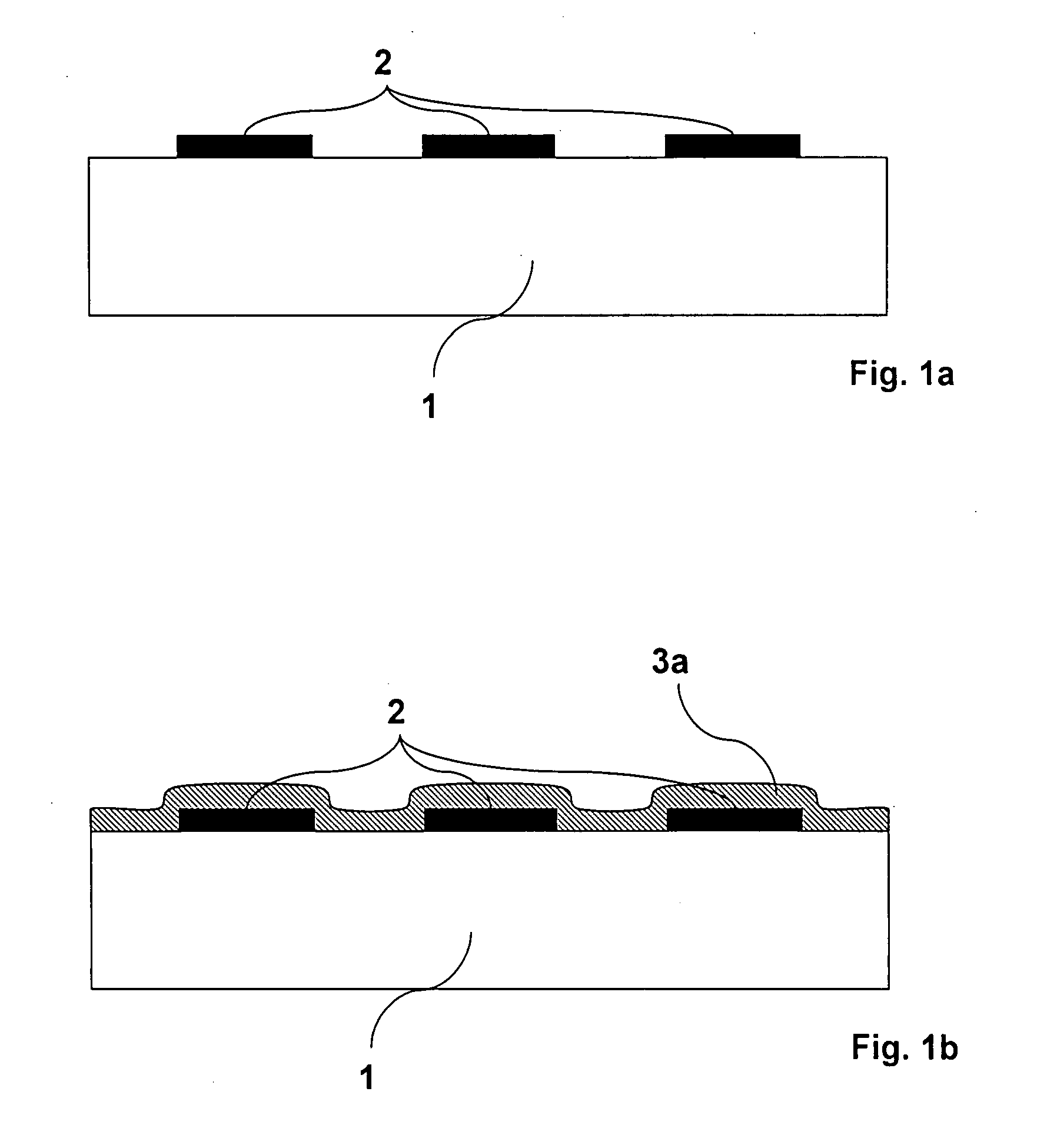
[0054]In the inventive method, the required resonance frequency of the resonators is set by varying the capacitances without varying the conductive structures (conductors). For this purpose, the resonator is coated with a dielectric material, the resonance frequency being determined by choosing the thickness of the dielectric layer.

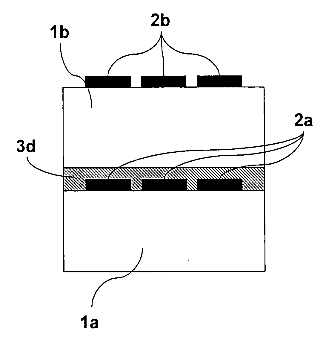
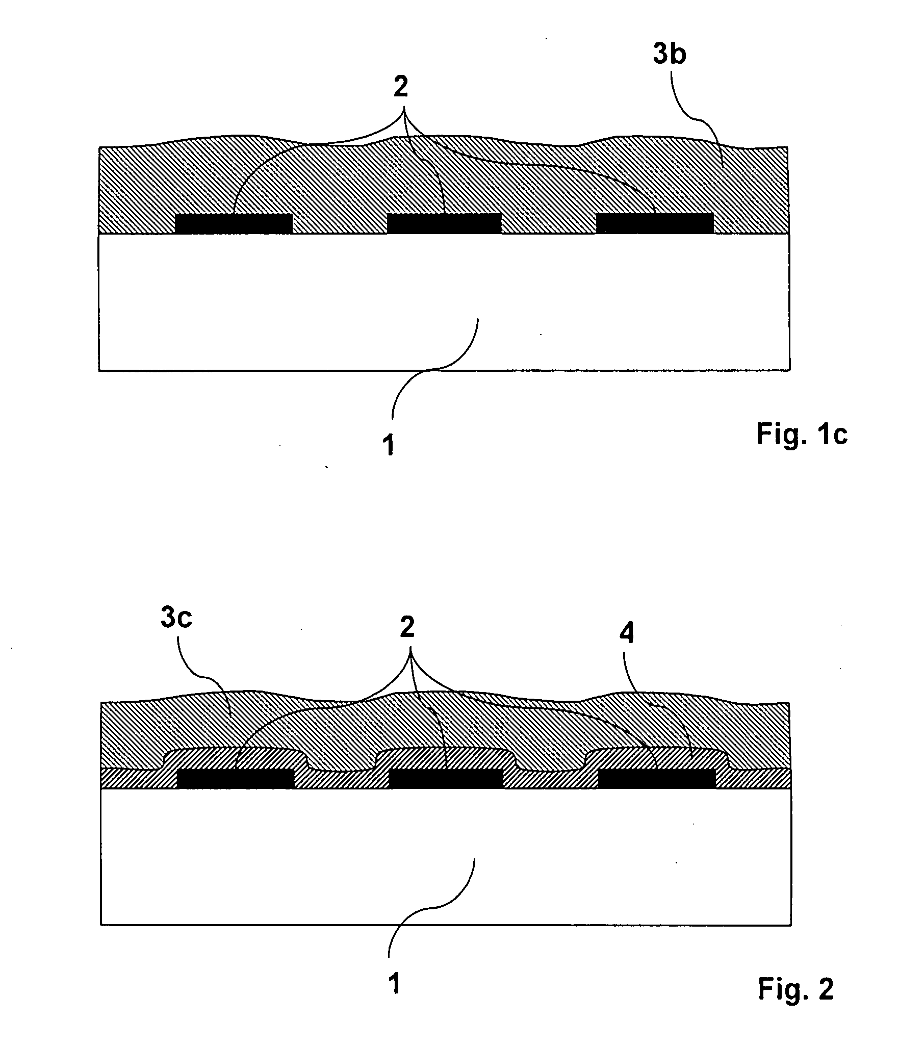
[0055]FIG. 1a shows a section through a substrate 1 and the conductive structures (conductors 2), e.g. within the finger capacitances of an HTS resonator or conductors of spiral resonators. FIG. 1b shows the corresponding resonator that is inventively coated with a dielectric layer 3a of little thickness. FIG. 1c shows an inventive resonator with a coating 3b with great thickness. For simple manufacturing, the inventive resonators, as shown in FIGS. 1b and 1c, are fully coated with a dielectric layer. However, it is possible to leave irrelevant regions uncoated.

[0056]In addition to the setting of the resonance frequency of the resonator system, the dielec...


PUM


Abstract

A radio-frequency (RF) resonator system, in particular, for a magnetic resonance (MR) probe, comprising at least one RF resonator with a substrate, on which a conductive structure is applied, wherein the conductive structure comprises regions of capacitive and inductive elements, is characterized in that the conductive structure is coated at least in the regions of the capacitive elements with at least one dielectric layer that covers the regions of the capacitive elements at least partially, wherein the local thickness of at least one of the dielectric layers is set in dependence on the resonance frequency of the uncoated RF resonator, on a defined resonance frequency of the resonator once it is coated, on the dielectric constant of the substrate and on the dielectric constant of the materials of the dielectric layers. The inventive resonator system can be set to the required resonance frequency quickly, at low cost, reversibly, and with high precision and at the same time the dielectric strength of the resonator system is increased.

Description

[0001]This application claims Paris Convention priority of DE 10 2006 053 472.7 filed Nov. 14, 2006 the complete disclosure of which is hereby incorporated by reference.BACKGROUND OF THE INVENTION[0002]The invention relates to a radio-frequency (RF) resonator system, in particular, for a magnetic resonance (MR) probe, comprising at least one RF resonator with a substrate, to which a conductive structure is applied, wherein the conductive structure comprises areas with capacitive and inductive elements. Moreover, the invention relates to a method for tuning such an RF resonator system.[0003]Such RF resonator systems are known from [7] and the references cited therein.[0004]For MR applications, RF resonator systems are used to irradiate RF pulses and detect RF signals from the measurement samples. An RF resonator system can comprise one or more RF resonators. In the case of high-resolution MR apparatus, the sensitivity of the apparatus can be increased by using high-temperature superc...

Claims


Application Information

Patent Timeline
IPC IPC(8): G01V3/14G01V13/00H01L39/00
CPCG01R33/34007G01R33/34023G01R33/3628G01R33/34092G01R33/341G01R33/34061H01Q7/005
Inventor FREYTAG, NICOLAS
Owner BRUKER SWITZERLAND AG
Why Eureka
Try Eureka