Electromagnetic Wave Shielding Grid Polarizer and Its Manufacturing Method and Grid Polarizer Manufacturing Method

a technology of electromagnetic wave shielding and grid polarizer, which is applied in the direction of polarising elements, instruments, other domestic objects, etc., can solve the problems of affecting the image expression, wrong operation of peripheral instruments, and flickering of image expression on the panel, so as to reduce thickness, suppress electromagnetic radiation, and low cost

Inactive Publication Date: 2008-05-22
ZEON CORP
View PDF3 Cites 43 Cited by
  • Summary
  • Abstract
  • Description
  • Claims
  • Application Information

AI Technical Summary

Benefits of technology

[0059] The electromagnetic wave shielding grid polarizer according to the present invention has a polarizing function combined with a magnetic wave shielding function, and therefore, a liquid crystal display capable of suppressing electromagnetic radiation can be realized with a reduced thickness. The electromagnetic wave shielding grid polarizer can be provided in other optical elements, and a liquid crystal display can be made at a low cost. An electromagnetic wave shielding grid polarizer with a large area can be made in a low cost by the making process according to the present invention.
[0060] Further, by the process for making a grid polarizer according to the present invention, a grid polarizer having fine gratings with a size of sub-micron order and having a large area can be made in a low cost by adopting precision fine work and vapor deposition.

Problems solved by technology

For example, electromagnetic waves generated from a plasma display tend to cause wrong operation of peripheral instruments, and therefore, the plasma display is usually provided with a magnetic wave shielding sheet.
It is said that electromagnetic waves are also generated from a backlight of a liquid crystal display, and give an adverse influence on the image expression.
Especially a direct type backlight requiring high luminance generates intensive electromagnetic waves, and therefore, flicker in image expression on the panel occurs unless an electromagnetic wave shielding sheet is provided.
However, the provision of an electromagnetic wave shielding sheet over the direct type backlight is costly, and tends to cause another problem of taking foreign matter in the backlight system because of complexity of the system.
However, the operation of inserting the transferring foil in the mold for each shot of injection molding is complicated.
Further, this method can be adopted for injection molding, but cannot be adopted for a filmy grid polarizer suitable for a liquid crystal display.
However, the wire grid polarizer only with the pattern of parallel lines is not suitable for electromagnetic wave shielding.
The above-proposed processes wherein a photoresist or a polymethyl methacryalte this Film is exposed and developed, have a problem in that the side faces of the grids formed by development are not smooth, and hence, the optical properties of resulting grid polarizer are not satisfactory.
Further, a large-size grid polarizer is difficult to make.

Method used


Image

  • Electromagnetic Wave Shielding Grid Polarizer and Its Manufacturing Method and Grid Polarizer Manufacturing Method
  • Electromagnetic Wave Shielding Grid Polarizer and Its Manufacturing Method and Grid Polarizer Manufacturing Method
  • Electromagnetic Wave Shielding Grid Polarizer and Its Manufacturing Method and Grid Polarizer Manufacturing Method

Examples


example 1

[0242] Single crystal diamond rectangular parallelepiped with a size of 0.2 mm×1 mm×1 mm was soldered to an SUS shank having a size of 8 mm×8 mm×60 mm. A face having a size of 0.2 mm×1 mm of the single crystal diamond rectangular parallelepiped was subjected to a focused ion beam treatment using argon ion beams by a focused ion beam treating apparatus “SMI3050” available from Seiko Instruments Inc. whereby a plurality of grooves having a width of 0.1 μm, a depth of 0.1 μm and a pitch of 0.2 μm and extending parallel to the side of 1 mm length were formed. A cutting tool having 1,000 linear protrusions having a width of 0.1 μm, a height of 0.1 μm and a pitch of 0.2 μm was manufactured from the focused ion beam-treated diamond.

[0243] A stainless steel SUS 430 member having a size of 152.4 mm width×203.2 mm length×10.0 mm thickness was subjected to nickel-phosphorus electroless plating whereby a metal deposit layer having a thickness of 100 μm was formed on the face of 152.4 mm width×...

example 2

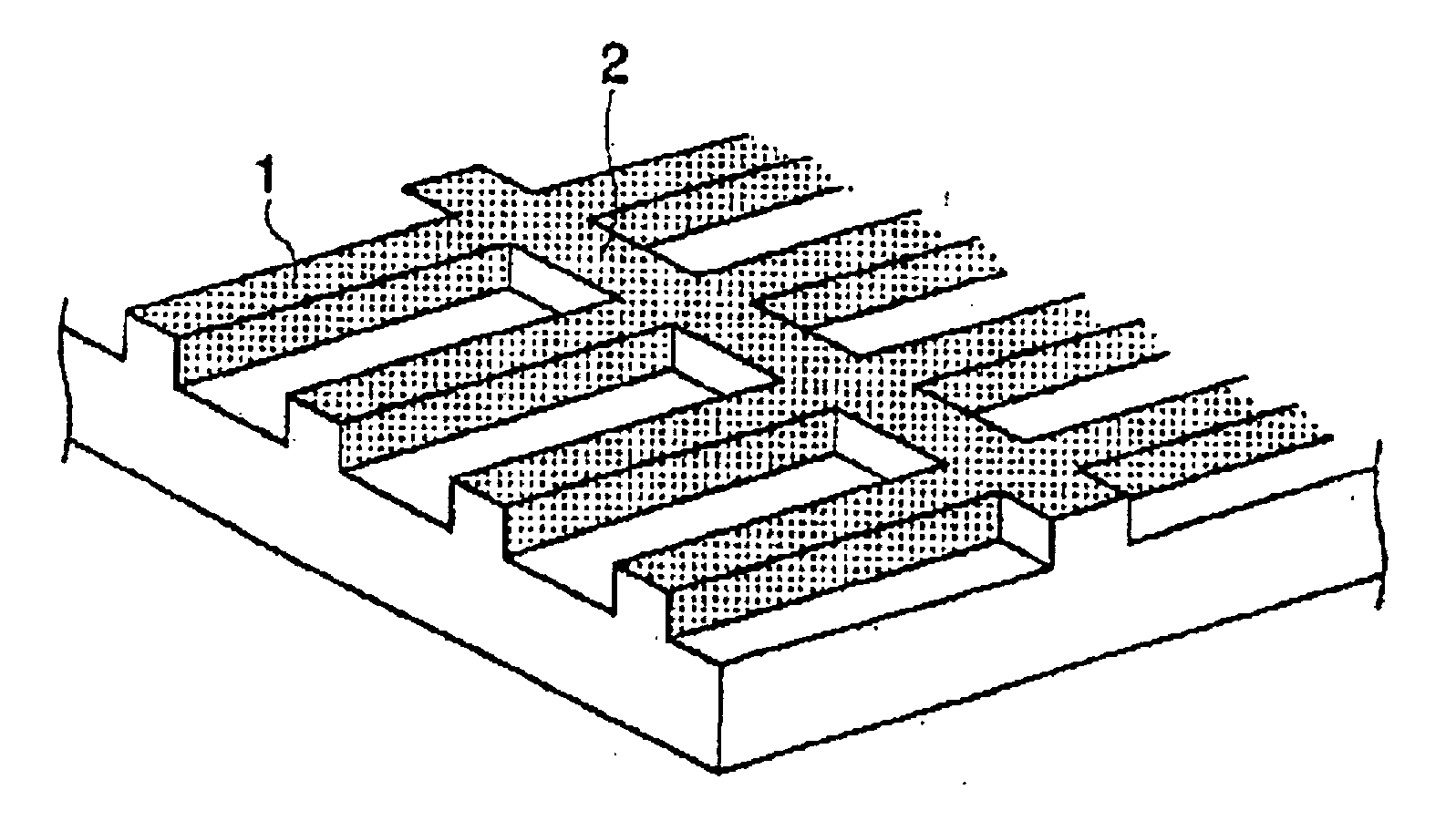
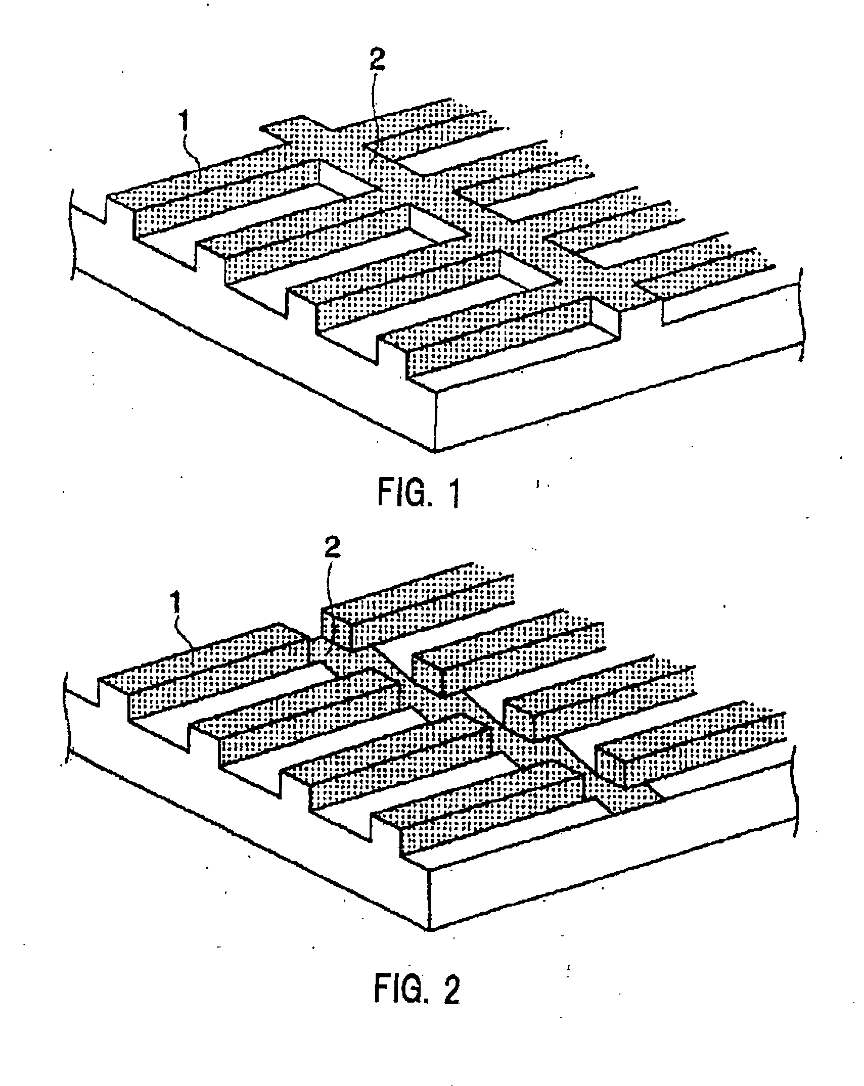
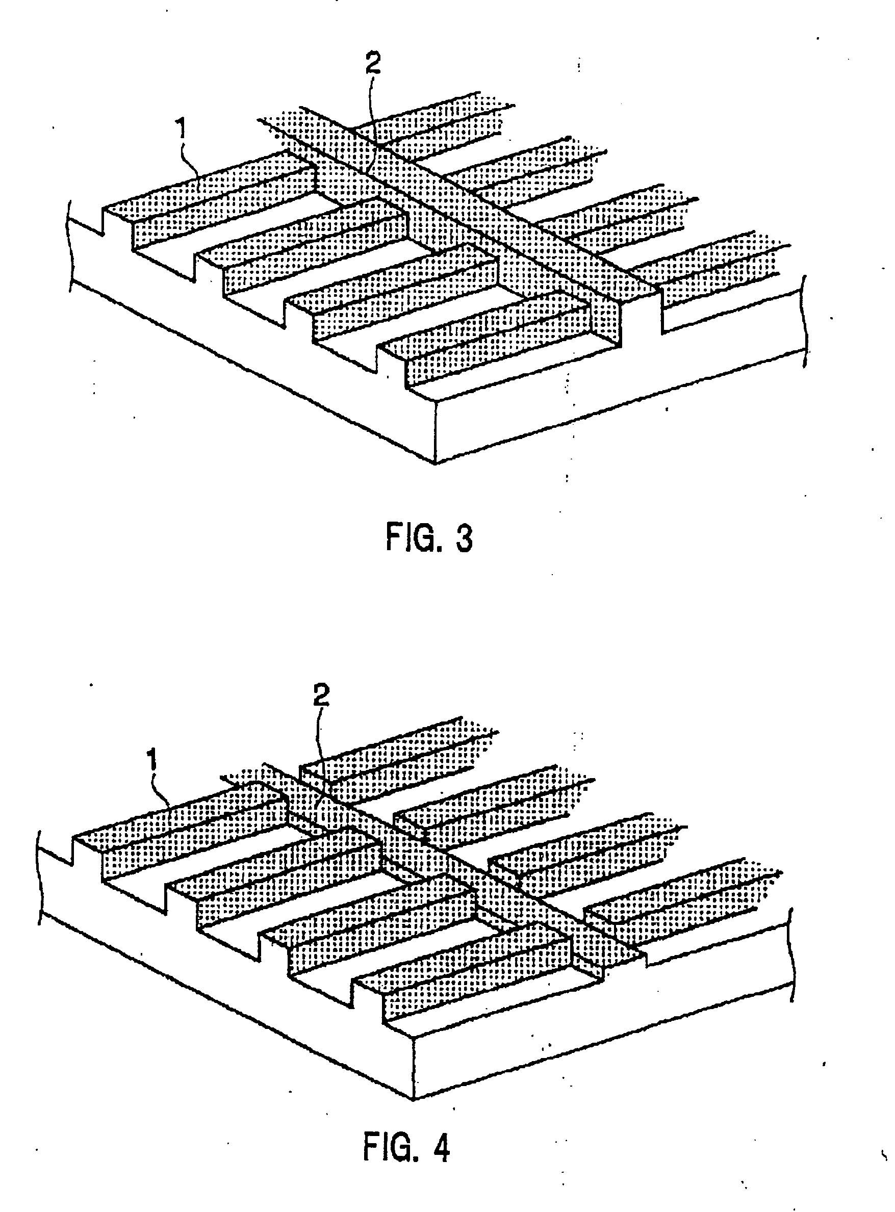
[0250] The entire curved surface of a stainless steel SUS 430 cylinder having a diameter of 200.0 mm and a height of 155.0 mm was subjected to nickel-phosphorus electroless plating to form a metal deposit layer having a thickness of 100 μm. Using the same cutting tool having linear protrusions as used in Example 1 and a precision fine working machine, the metal deposit layer was cut to form a fine grating shape consisting of linear grooves having a width of 0.1 μm, a depth of 0.1 μm and a pitch of 0.2 μm, and extending in a straight line and parallel to the end faces of the cylinder.

[0251] Using a single crystal diamond bite, the metal deposit layer was further cut to form a second grating shape consisting of gratings having a width of 10 μm, a depth of 0.5 μm and a pitch of 1 mm, and extending in a straight line and in the direction perpendicular to the linear grooves constituting the fine grating shape.

[0252] A resin having an alicyclic structure (“ZEONOR 1420R” available from Z...

example 3

[0255] A metal mold member having the fine grating shape and the second grating shape was prepared by the same procedures as mentioned in Example 1. The metal mold member was subjected to metal forming using an aqueous nickel sulfamate solution to form a thin nickel film with a thickness of 300 mm. The nickel film was peeled from the metal mold member to prepare a nickel film having transferred thereto the fine grating shape and the second grating shape. The nickel film was inserted in a mold for injection molding, and the resin having an alicyclic structure was injection-molded. By the same procedures as mentioned in Example 1, an electromagnetic wave shielding grid polarizer was manufactured.

[0256] The polarized light transmittance and the electromagnetic wave shielding performance of the electromagnetic wave shielding grid polarizer were evaluated. S-polarized light transmittance was 60.3%, p-polarized light transmittance was 0.3% and thus the polarized light transmittance diffe...


PUM

PropertyMeasurementUnit
widthaaaaaaaaaa
widthaaaaaaaaaa
heightaaaaaaaaaa

Abstract

An electromagnetic wave shielding grid polarizer wherein a fine grating shape (1) consisting of linear, parallel projecting gratings and a grating shape (2) consisting of parallel gratings crossing fine grating shape (1) and having 0.1-500 μm width and 1 μm-100 nm pitch are formed; the total length of portions having lengths 10−5 to l0−1 times the wavelength of electromagnetic wave is at least 80% out of the projecting gratings of fine grating shape (1) segmented by the gratings of grating shape (2); and fine grating shape (1) is electrically interconnected with grating shape (2) by a conductive reflective material. The grid polarizer is made by a method of transferring linear, parallel grooves of a metal mold or a metal film to a transparent resin shaped article, and vapor-depositing a conductive reflective material on the shaped article, or by a method of formation of a conductive reflective material layer on a transparent base, coating with a resist, exposure to active radiation, development and etching.

Description

TECHNICAL FIELD [0001] This invention relates to an electromagnetic wave shielding grid polarizer, and a method of making the same, and a method of making a grid polarizer. Yore particularly, this invention relates to a grid polarizer having a function of shielding electromagnetic waves adversely influencing electronic parts, and a method of making the grid polarizer having a large area at a reduced cost, and a method of making a grid polarizer having fine gratings with a size of a submicron order and having a large area at a reduced cost by precision working and vapor deposition. BACKGROUND ART [0002] In recent years, electromagnetic wave-generating instruments such as a large size television set, a display of a personal computer, and a cell phone have been popularly used. Great attention is attracted for shielding electromagnetic waves. For example, electromagnetic waves generated from a plasma display tend to cause wrong operation of peripheral instruments, and therefore, the pla...

Claims


Application Information

Patent Timeline
Patent Type & Authority Applications(United States)
IPC IPC(8): G02B5/30B05D5/06B29D11/00
CPCG02B5/3058G02B5/30
Inventor HAYASHI, MASAHIKOOOISHI, HITOSHI
Owner ZEON CORP
Why Eureka
Try Eureka