Personalized hardware

a technology of integrated circuits and hardware, applied in the direction of photomechanical equipment, instruments, semiconductor/solid-state device details, etc., can solve the problems of inadequacies of visual identification solutions, high cost of nvm solutions, and inability to meet the needs of users, etc., to achieve high manufacturing throughput, high manufacturing efficiency, and low cost. , the effect of high manufacturing efficiency

Inactive Publication Date: 2008-05-22
MANGELL EFRAIM
View PDF67 Cites 27 Cited by
  • Summary
  • Abstract
  • Description
  • Claims
  • Application Information

AI Technical Summary

Benefits of technology

[0044]In a preferred embodiment, the present invention seeks to provide an apparatus and method to implement these features in a highly flexible, secure, cheap, reliable and manufacturable manner, reducing the above-mentioned problems of the prior art.
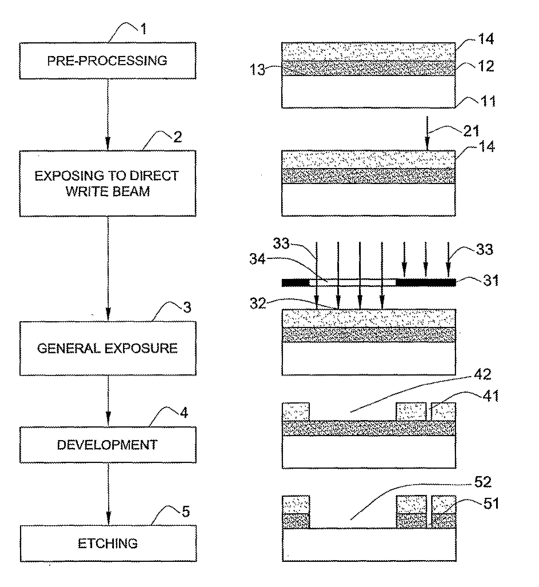
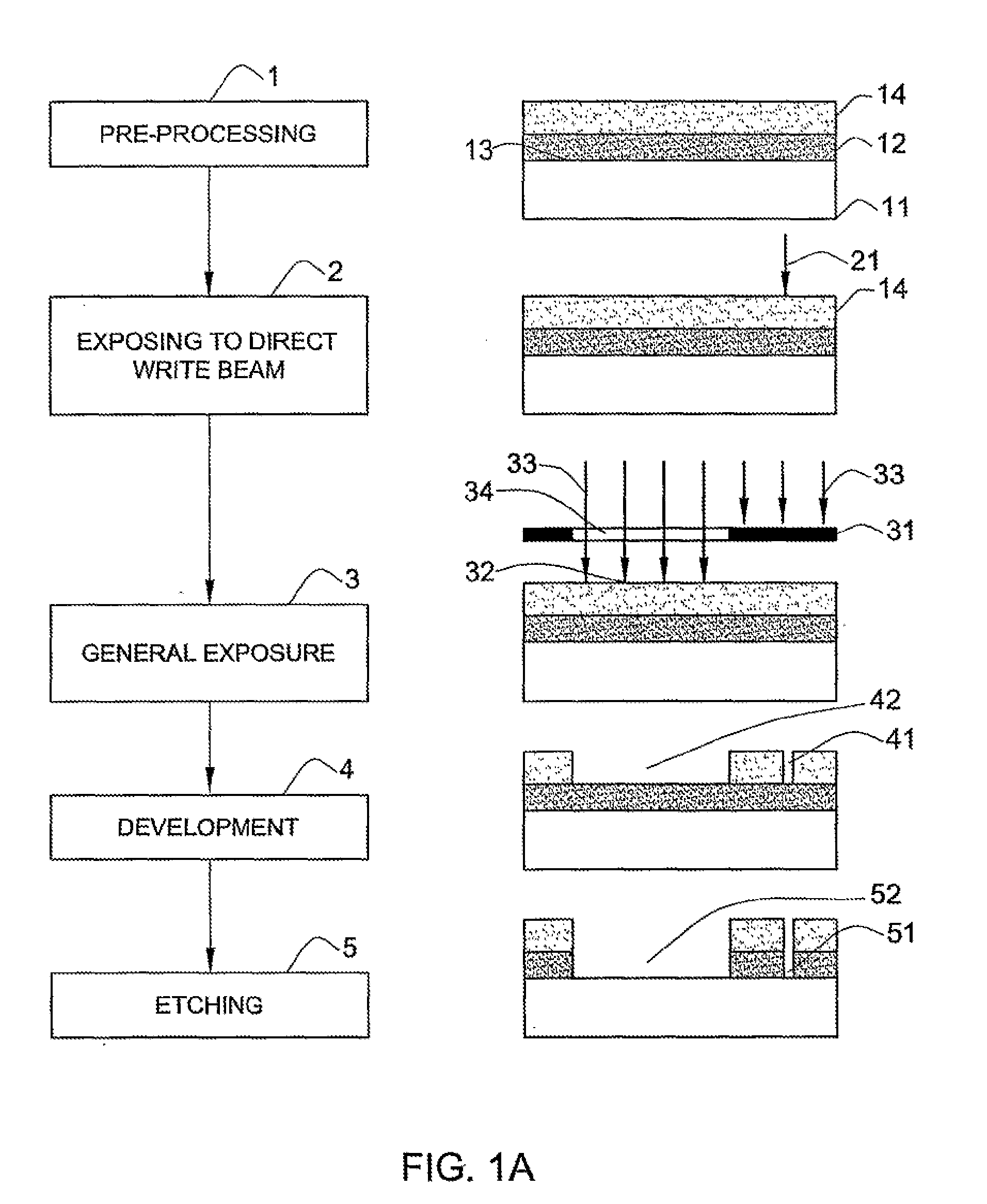
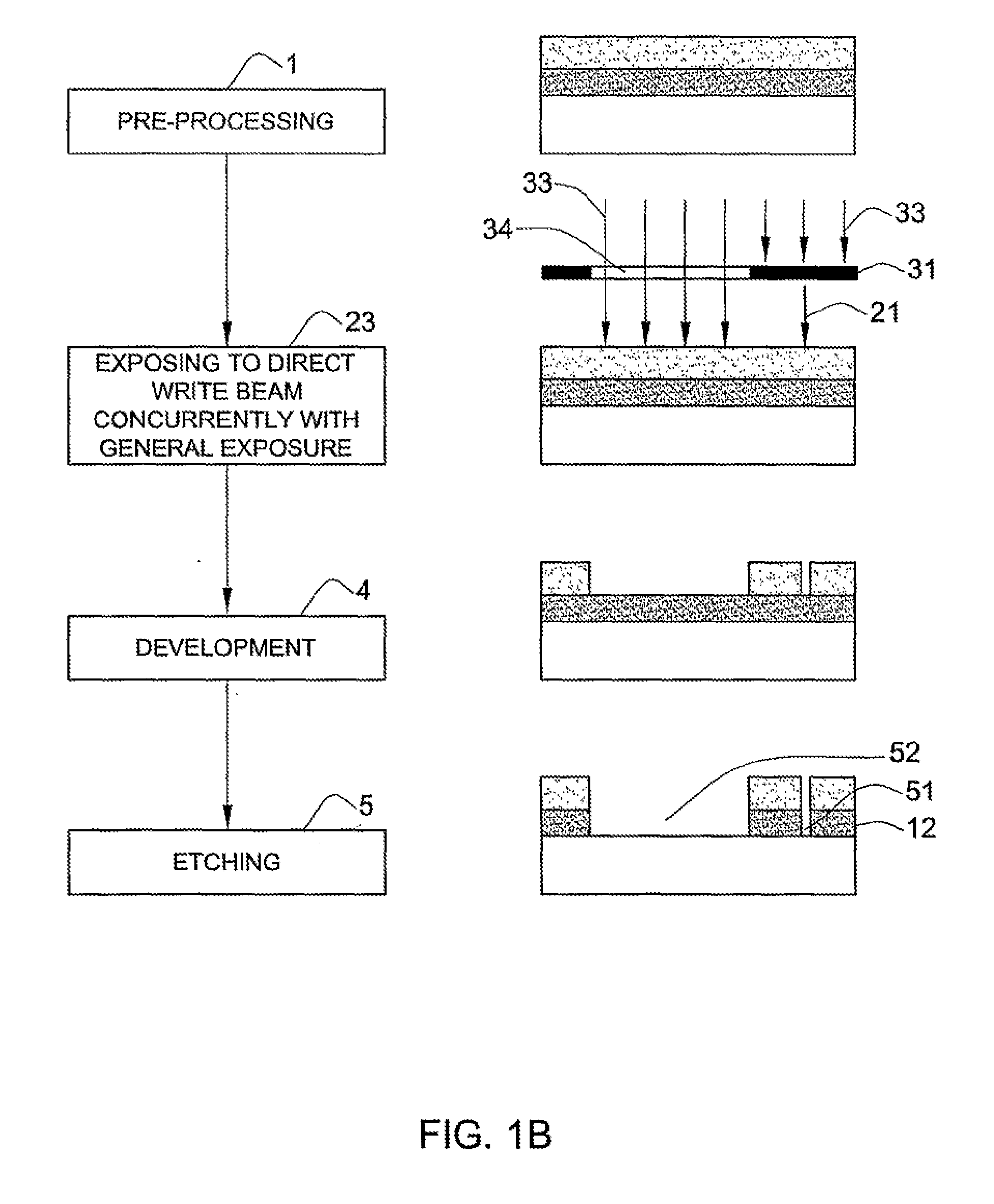
[0045]In a preferred embodiment of the present invention, defining chip specific electrical circuits serving as a digital number (which may be used, for example, for serial and ID numbers, keys) while maintaining high manufacturing throughput, low cost, flexibility, security and quality is achieved by combining optical parallel lithography with another specific lithography technique on photoresist.
[0046]Some methods described in the prior art combine optical lithography with e-beam lithography. These patents seek to cope with the throughput constraints posed by using e-beam lithography, as perceived in applications requiring the direct write of high-resolution on-chip devices, by combining optical parallel lithography with e-beam direct write. However, it will be appreciated by persons skilled in the art that a method which is capable of achieving further improved throughput would be highly desired in some applications. The present invention seeks to provide, in a preferred embodiment comprising an improved combination of optical parallel lithography with another type of lithography such as e-beam lithography or laser direct write lithography, further improved throughput and processing advantages as well as improved security. Any of the various processes for determining electrical characteristics of a layer of an electrical circuit (such as, for example, optical parallel lithography, or any other type of lithography as discussed above) is also termed herein an electrical characteristic determination process (ECDP).
[0075]In accordance with another aspect of the invention exposing of the PSH links is accomplished by using a PSH photo-mask. By a preferred embodiment of this aspect of the invention, said photo-mask is used (within the same scanner system) in addition to a parallel lithographic stepping exposure utilizing a general photo-mask that is common for all the chips. Such a PSH photo-mask is dedicated to expose into the photo-resist an individualized pattern achieving a similar result to that achieved by direct write but in a different manner, in this case by masking the full optical light beam and allowing only a spot beam to pass through and bring a spot of appropriate shape and dimensions to the photoresist surface, as further described below. In accordance with another preferred embodiment of this aspect of the invention, the PSH photomask is combined with the general photomask such that, outside the normal exposure field, there is a shape or a plurality of shapes to allow for the spot beam exposure in a second double-exposure. The reticle (mask) is off-set to direct the beam through this shape instead of the general field, while letting through only the spot beam. This method obviates the necessity of exchanging reticles, and thus improves production throughput.
[0122]According to a preferred embodiment of the present invention the key to be incorporated into a specific chip by utilizing the PSH technique may be calculated with an algorithm utilizing one or more specific manufacturing parameters, such as lot number, wafer number and die x-y coordinates (seed) that individually defines each chip. Algorithms may vary for different chip layers to enhance security.
[0124]By a preferred embodiment, algorithms may vary for different layers to enhance security.

Problems solved by technology

In several ways, the prior art solutions as described above have significant drawbacks.
In systems where electrical functionality is required, for example, in which the readout of the different identification details from the chip or their content is influencing the results of some algorithms, visual identification solutions are not appropriate.
The EPROM, EEPROM, FLASH and other similar NVM solutions all require costly extra processing, for on-chip high voltage circuitry, tunnel oxide, floating poly gate, etc., typically adding up to 4 or 5 additional mask layers.
Also, the NVM requires extensive extra silicon area.
And additionally, the NVM is difficult to integrate with pure logic processes, for performance and quality reasons, and therefore tends to hold back the process technology by one or two generations.

Method used


Image

  • Personalized hardware
  • Personalized hardware
  • Personalized hardware

Examples


example 1

[0202]FIGS. 5-6 show an example of alteration of functioning of electrical circuits by individually expose its elements during the lithography process, in the manner that was, described above. A state of an inverter gate circuit 601 (in this example, part of a Pull-Down Register) may be changed from “1” to “0” by exposing the photoresist corresponding to a polygon in the metal layer of a conductor 602 shown in the electrical schematics of the circuit. By following this approach a series of bits that correspond to a digital key can be incorporated into the chip.

[0203]Consider, for example, an 8-bit inverter array (functioning as, for example, a digital key) built up from 8 of the gate circuits 601 (the layout of the metal and contact layers as shown in FIG. 6). As will be appreciated by persons skilled in the art, by selectively exposing the photo-resist to a direct write beam or by exposing the photoresist through a special PSH photo-mask, as described above, the corresponding PSH l...

example 2

[0206]The PSH technique can be used for personalization of a ROM. FIG. 7 shows a schematic 401 and a layout 402 of a Vt implant ROM realizing a Truth Table 403, that is personalized according to the invention. By using the PSH technique, the transistor gate locations 412 on the circuit corresponding to the requested combination of the transistors (e.g. those designated 413) are selectively exposed on the photo resist in order to form PSH links and thereby enabling Vt (threshold voltage) implant during manufacture of the chip. The presence or absence of the Vt implant, as individually defined during the PSH exposure of each chip, will implement respectively the logic ‘1’s and ‘0’s in the ROM truth table, different in every chip.

example 3

[0207]According to a preferred embodiment, special care can be taken for security applications to layout the PSH links to make them visually identical to circuits that do not contain PSH links. FIG. 8 shows an example of alteration of a characteristic of an electrical circuit 501 corresponding to a logic NOR gate (diagram 502). After the alteration by utilizing the PSH technique the NOR gate circuit 501 effectively transforms into a circuit 503 corresponding to of a logic NAND gate (diagram 504). During the chip manufacture, by selectively forming the PSH links, and thereby enabling or blocking Vt implant, two transistors 511 of the electrical circuit 501 are effectively cancelled. The circuit visually looks like a NOR gate, but effectively behaves like a NAND gate. This may be good for security purposes, making reverse engineering more difficult.

[0208]Combining a multitude of such gates, for example, and selectively exposing them will enable implementation of digital keys and numbe...


PUM

PropertyMeasurementUnit
electrical characteristicsaaaaaaaaaa
electrical characteristic determinationaaaaaaaaaa
electrical characteristicaaaaaaaaaa

Abstract

A system for personalizing one or more electrical circuits having plurality of layers with electrical characteristics. The layers being produced by an electrical characteristic determination process (ECDP). The system for personalizing includes a wafer stage for receiving a wafer in order to produce a plurality of electrical circuits. The system is configured to apply a personalization process during production of the layers. The personalization process includes using a first ECDP in the layer to product identical electrical characteristics on the wafer in each of the plurality of electrical circuits, and using a second ECDP in the layer to modify one or more electrical characteristics in selected electrical circuits so as to incorporate in the selected circuits an individualized digital number, giving rise to the desired personalizing of one or more of the specified electrical circuits. Related apparatus and methods are also provided.

Description

CROSS REFERENCE TO RELATED APPLICATIONS[0001]The present application is a continuation application based upon application Ser. No. 10 / 181,518, filed Dec. 16, 2002.FIELD OF THE INVENTION[0002]The present invention relates to design and manufacture of integrated circuits (ICs) and, more specifically, to apparatus and methods for personalizing ICs.BACKGROUND OF THE INVENTION[0003]In the semiconductor industry, there is a need to enable differentiation between single chips for purposes, for example, of: manufacturing control; tracking of the chips' history; and identification and serial numbers in various applications.[0004]The semiconductor manufacturing process for mass production in general is based upon methods for making a large number of “many-of-the-same” chips, and therefore, to differentiate between chips effectively and efficiently without compromising the manufacturing throughput capacity, cost and quality is a major challenge.[0005]Depending on the purpose for the differenti...

Claims


Application Information

Patent Timeline
Patent Type & Authority Applications(United States)
IPC IPC(8): G06F19/00G03F1/14G03F7/20H01L21/8247H01L27/02H01L27/115
CPCG03F7/2022H01L23/544H01L27/02H01L2223/54433H01L2223/5444H01L2924/0002G03F1/00H10B41/00H10B69/00H01L2924/00G03F1/62
Inventor MANGELL, EFRAIM
Owner MANGELL EFRAIM
Why Eureka
Try Eureka