

Avalanche Photodiode
a photodiode and low-darkcurrent technology, applied in the field of low-darkcurrent avalanche photodiodes, can solve the problems of low yield rate, insufficient suppression effect, and increase production cost, and achieve high long-term reliability, small dark current, and simple process
- Summary
- Abstract
- Description
- Claims
- Application Information
AI Technical Summary
Benefits of technology
Problems solved by technology
Method used
Image

Examples
embodiment 1
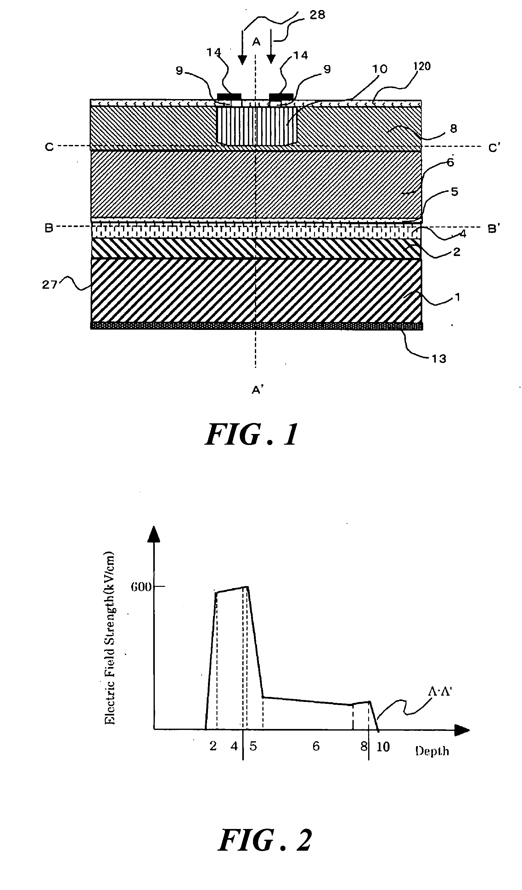
[0055]FIG. 1 is a cross-sectional view schematically illustrating a structure of an avalanche photodiode according to Embodiment 1 of the present invention. In the avalanche photodiode according to Embodiment 1, the n-type as a first conductivity type, the p-type as a second conductivity type, an n electrode as a first electrode, and a p electrode as a second electrode are utilized. The production of the respective semiconductor layers can be realized on a wafer-like substrate 1 made of an n-type InP or the like, by utilizing the MO-CVD, the molecular beam epitaxial (MBE) growth method, or the like. In Embodiment 1, the respective semiconductor layers were produced in accordance with the following order of steps: On a substrate 1, a first semiconductor layer 2 (hereinafter, referred to as a buffer layer) of an n-type InP having a carrier concentration of 0.2×1019 cm−3 to 2×1019 cm−3 or the like was grown as thick as 0.1 μm to 1 μm; an avalanche multiplication layer 4 of an i-type Al...
embodiment 2
[0064]In an avalanche photodiode according to Embodiment 2 of the present invention, in addition to the avalanche photodiode described in Embodiment 1, a transition layer 7 is provided between the light absorption layer 6 and the window layer 8. As the formation method for the transition layer 7, following to the step, in embodiment 1, in which the light absorption layer 6 is grown, for example, by growing an i-type GaInAsP to 0.01 μm to 0.05 μm in thickness, the transition layer 7 is formed.
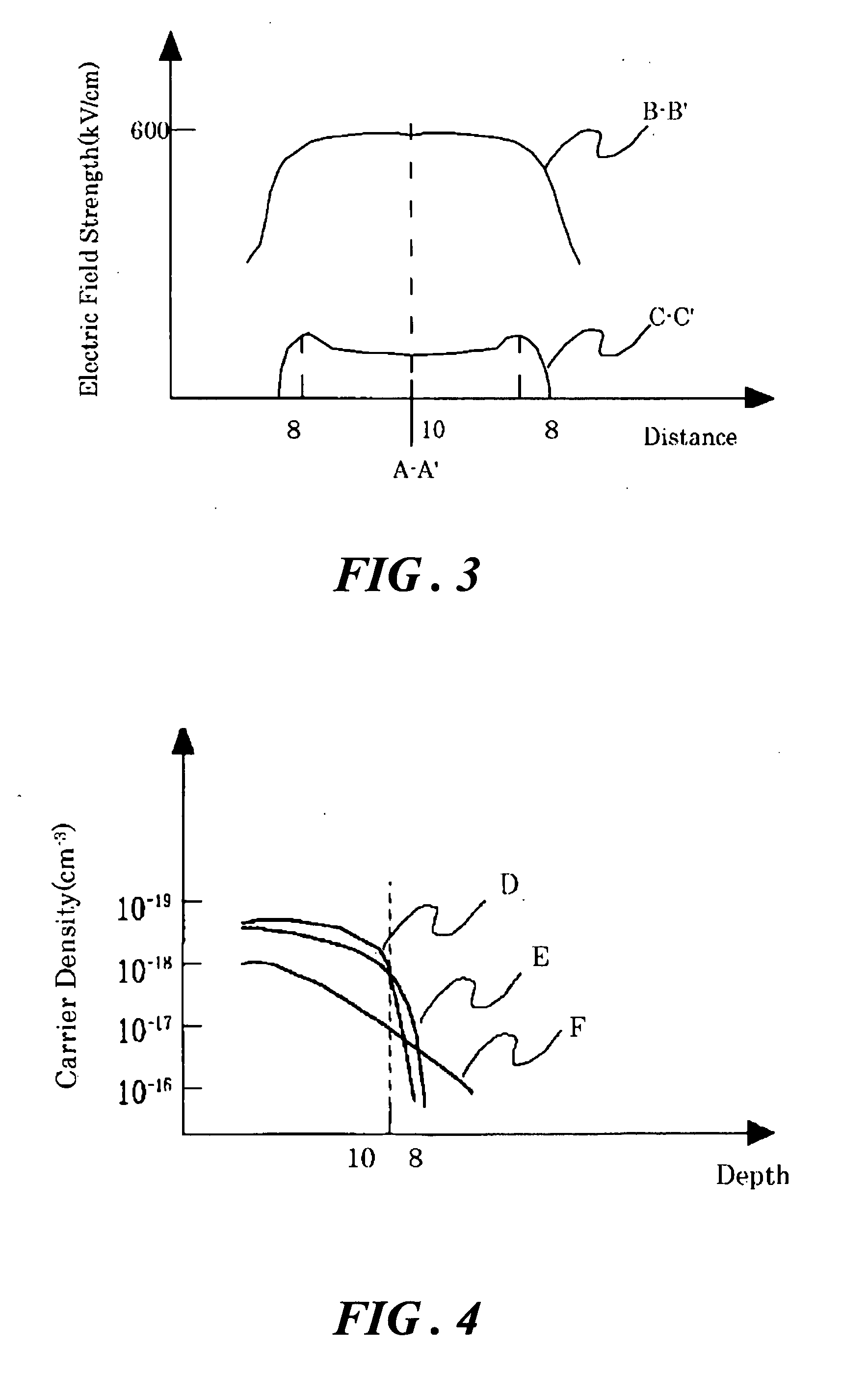
[0065]FIG. 5 is a graph representing the respective energy distributions, in the layer-junction portions, in a conductive band and a valence band in an avalanche photodiode according to Embodiment 2. The numerals along the abscissa and the ordinate denote the respective layered semiconductor layers and the energy, respectively; in FIG. 5, the character G, the character H, and the character I indicate the energy in the conductive band, the valence band, and the hole, respectively. It can be seen ...
embodiment 3
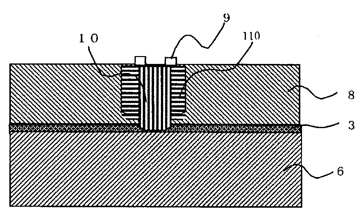
[0068]In an avalanche photodiode according to Embodiment 3 of the present invention, in addition to the avalanche photodiode described in Embodiments 1 and 2, a p-type peripheral conductive region 110 is provided around the p-type conductive region 10. FIGS. 6 and 7 are cross-sectional views each schematically illustrating a structure of an avalanche photodiode according to Embodiment 3 of the present invention. Reference numeral 6 denotes a light absorption layer; reference numeral 3 denotes a stopper layer which transits holes and stops the diffusion of holes. Reference Numerals 8 and 9 denote a window layer and a contact layer, respectively.
[0069]In an avalanche photodiode illustrated in FIG. 6, the p-type conductive region 110 is formed through shallow selective thermal diffusion performed in a wide area extending beyond the circumference of the contact layer 9, in such an extent as not to reach the transition layer 7, and then deep selective thermal diffusion is performed in an...
PUM
 Abstract
Description
Claims
Application Information