

Apparatus for manufacturing group iii nitride compound semiconductor light-emitting device, method of manufacturing group iii nitride compound semiconductor light-emitting device, group iii nitride compound semiconductor light-emitting device, and lamp
a technology of compound semiconductors and light-emitting devices, which is applied in the direction of chemically reactive gases, crystal growth processes, polycrystalline material growth, etc., can solve the problems of increasing the size of the sputter, difficult for the conventional sputtering method to finely adjust the doping density, and difficult to inject mg into the crystals, so as to reduce the size of the apparatus and optimize the density of the dopant element. , the effect of reducing the time required
- Summary
- Abstract
- Description
- Claims
- Application Information
AI Technical Summary
Benefits of technology
Problems solved by technology
Method used
Image

Examples
example 1
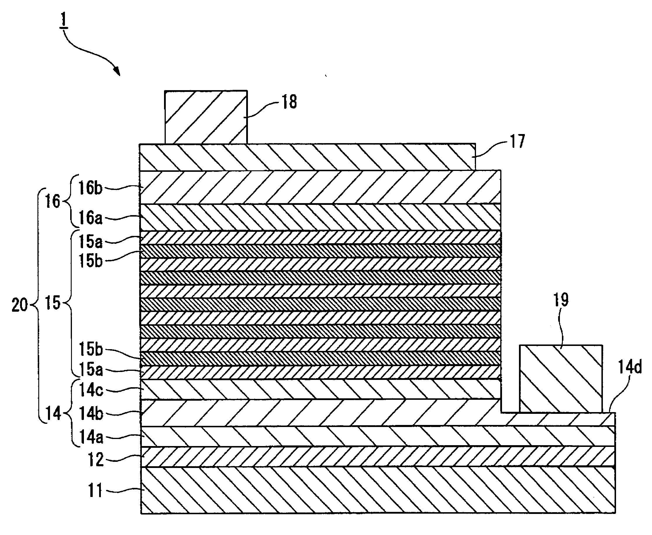
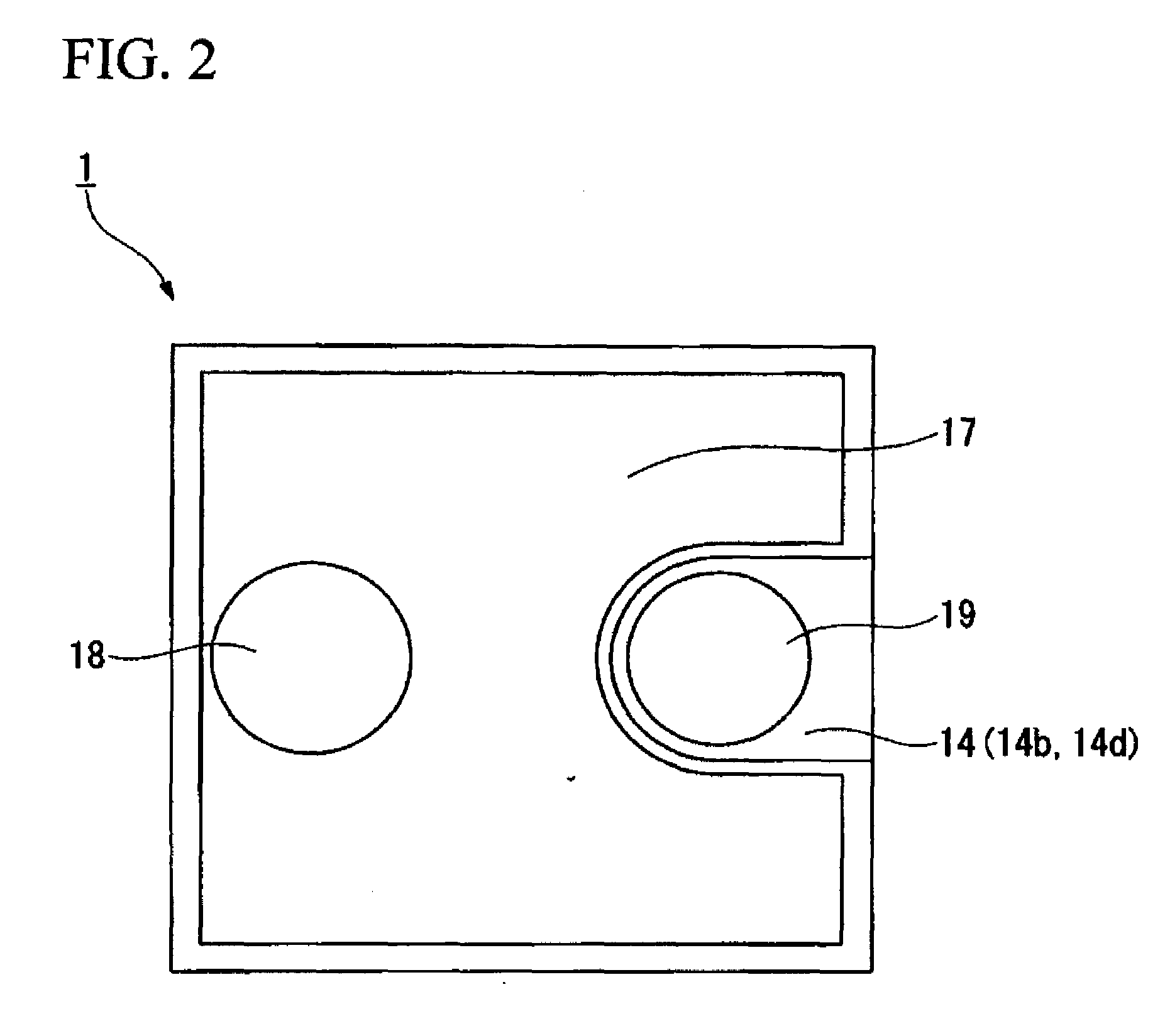
[0220]As described below, the laminated semiconductor 10 shown in FIG. 4 was manufactured and the light-emitting device shown in FIGS. 1 and 2 was manufactured.
[0221]First, the substrate 11 made of polished sapphire was prepared and subjected to pre-treatment as follows. That is, the substrate 11 was placed in a chamber for sputtering in which a target that is made of Al and is used to form the intermediate layer 12, the substrate 11 was heated at 500° C., and a nitrogen gas was introduced into the chamber at a flow rate of 15 sccm with the internal pressure of the chamber kept at 1.0 Pa. Then, an RF bias power of 50 W was applied to the substrate 11 without supplying power to the target, and a surface of the substrate 11 was cleaned by exposing the substrate 11 to nitrogen plasma.
[0222]After the pre-treatment, with the internal pressure of the chamber kept to 0.5 Pa, an argon gas and a nitrogen gas were introduced into the chamber at flow rates of 5 scam and 15 scam, respectively, ...
example 2
[0243]Using the light-emitting device manufacturing apparatus 50 shown in FIG. 6, under the same conditions as Example 1 except that the area ratio of the Ga target 47a to the dopant target 47b is 1:1 and the film forming conditions of the n type contact layer 14b are different, the laminated semiconductor 10 shown in FIG. 4 was manufactured and the light-emitting device shown in FIGS. 1 and 2 was manufactured.
[0244]More specifically, unlike Example 1, in Example 2, with the area of the Ga target 47a equal to the area of the dopant target 47b, the ratio of power applied to the Ga target 47a to power applied to the dopant target 47b was preset such that the density of Si in the n type contact layer 14b to be formed becomes 8×1018 cm−3. For example, RF power applied to the dopant target 47b was set to 1 / 100 of the RF power applied to the Ga target 47a, that is, 0.01 W / cm2. At this time, plasma was generated by the RF dielectric coupling plasma generator 22 provided within the chamber ...
example 3
[0247]Using the same light-emitting device manufacturing apparatus 40 shown in FIG. 3 as that in Example 1, under the same conditions as those in Example 1 except for tee area ratio (1:1) of the Ga target 47a to the dopant target 47b and the film forming conditions of the n type contact layer 14b, the laminated semiconductor 10 shown in FIG. 4 was manufactured and the light-emitting device shown in FIGS. 1 and 2 was manufactured.
[0248]More specifically, unlike Example 1, in Example 3, with the area of the Ga target 47a equal to the area of the dopant target 47b, the ratio of pulse applied to the Ga target 47a to pulse applied to the dopant target 47b was preset such that the density of Si in the n type contact layer 14b to be formed becomes 1.1×1019 cm−3. For example, a pulse of RF power applied to the dopant target 47b was set to 1 / 100 of the pulse of RF power applied to the Ga target 47a. That is, while the Ga target 47a is continuously supplied with power, the dopant target 47b w...
PUM
| Property | Measurement | Unit |
|---|---|---|
| Density | aaaaa | aaaaa |
| Ratio | aaaaa | aaaaa |
| Electric potential / voltage | aaaaa | aaaaa |
Abstract
Description
Claims
Application Information