Variable frequency oscillator and communication circuit with it

Inactive Publication Date: 2008-05-29
HITACHI LTD
View PDF15 Cites 30 Cited by
  • Summary
  • Abstract
  • Description
  • Claims
  • Application Information

AI Technical Summary

Benefits of technology

[0027]According to the invention, as the environment variation of the variable frequency oscillator can be compensated when a des

Problems solved by technology

The phase noise means the variation of a phase of an oscillation signal caused due to the thermal noise and the flicker noise of elements configuring the oscillator.
However, as an inductor the parasitic series resistance of which is small is required in the LC oscillator the phase noise of which is small, relative

Method used


Image

  • Variable frequency oscillator and communication circuit with it
  • Variable frequency oscillator and communication circuit with it
  • Variable frequency oscillator and communication circuit with it

Examples


Example

First Embodiment

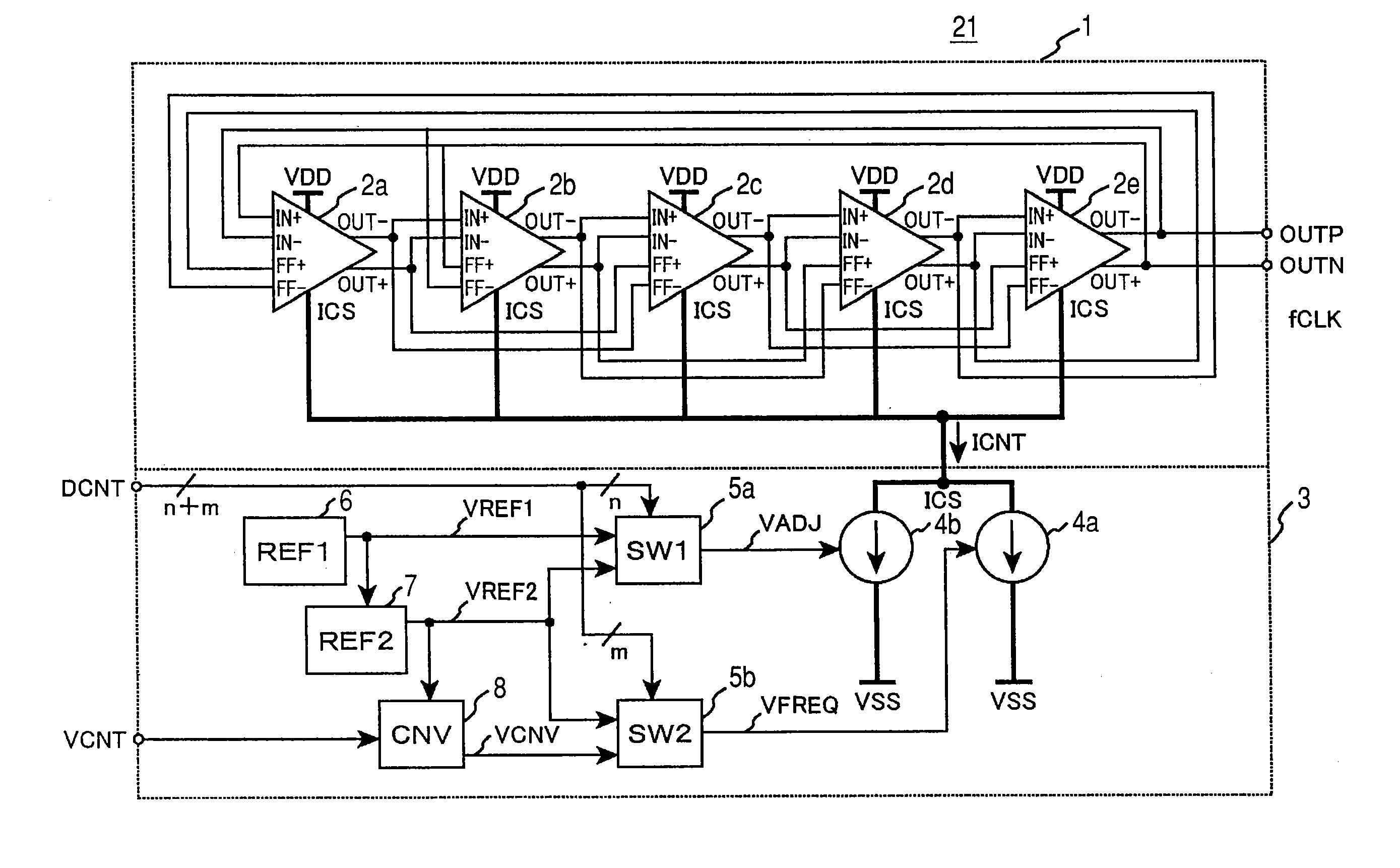
[0054]Referring to FIGS. 1 to 5, a first embodiment of a variable frequency oscillator according to the invention will be described below.

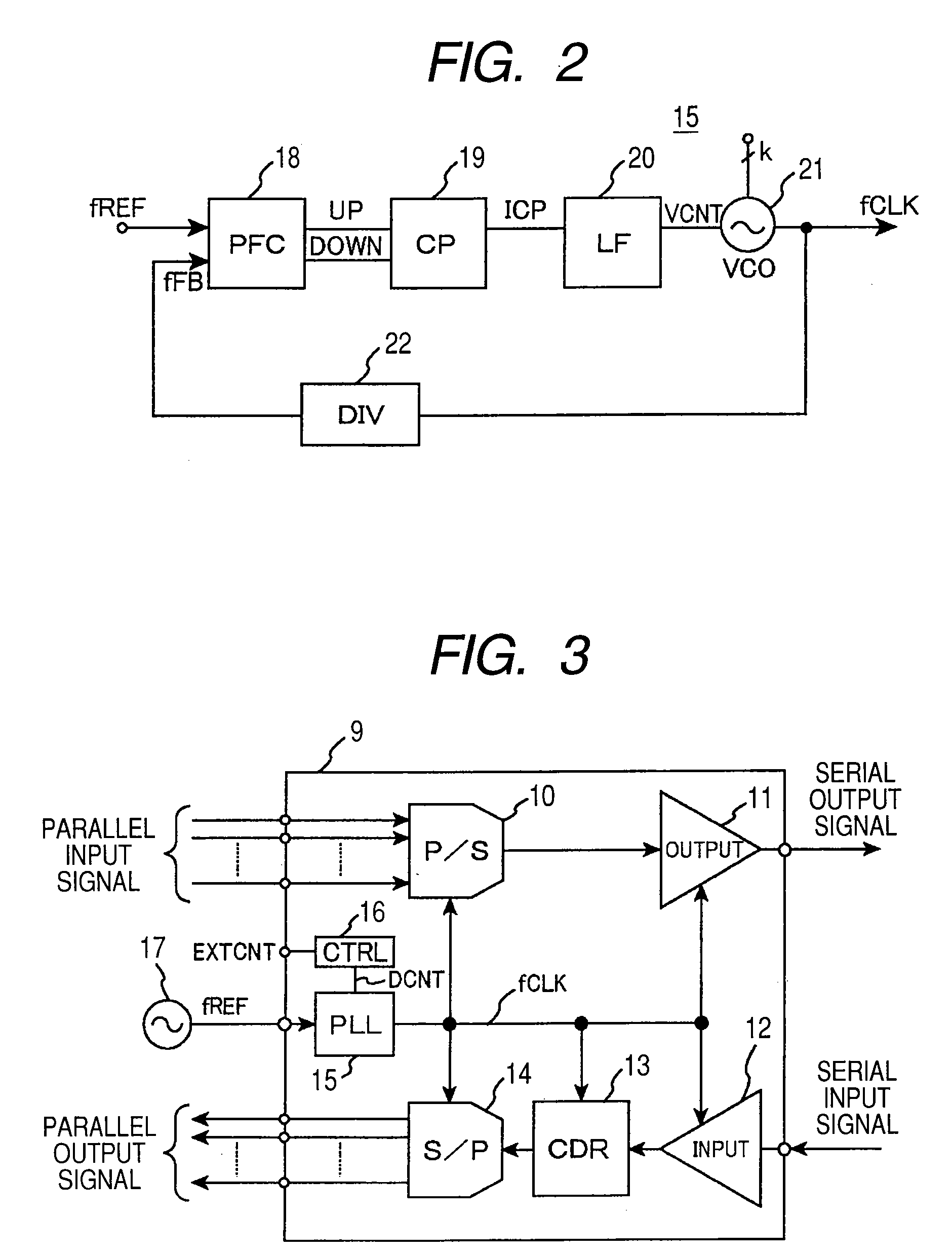
[0055]First, FIG. 2 shows an example of the configuration of PLL in which the variable frequency oscillator according to the invention is used. The PLL 15 includes a phase frequency detector (PFC) 18, a charge pump (CP) 19, a loop filter (LF) 20, a voltage controlled oscillator (VCO) 21 and a divider (DIV) 22. The phase frequency detector (PFC) 18 compares phase difference between a reference clock signal of a frequency fREF and a feedback clock signal fFB acquired by dividing an output signal by the divider and outputs an up pulse when the feedback signal lags the reference clock signal or a down pulse when the feedback signal leads. The charge pump 19 outputs current ICP according to the input up or down signal and charges or discharges the capacity of the loop filter 20. An output terminal of the loop filter 20 is connected to a...

Example

Second Embodiment

[0081]Next, for a second embodiment of the invention, referring to FIGS. 6 to 8, an example of the practical configuration of a voltage-to-current conversion circuit 3 of a variable frequency oscillator 21 will be described.

[0082]The voltage-to-current conversion circuit 3 is provided with a reference voltage source circuit 30 corresponding to the reference voltage source circuit (REF1) 6, a reference voltage conversion circuit 31 corresponding to the reference voltage conversion circuit (REF2) 7, a voltage conversion circuit for frequency control 32 corresponding to the voltage conversion circuit for frequency control (CNV) 8, voltage select switch circuits 33, 34 corresponding to the first and second voltage select switch circuits 5 (5a, 5b) and voltage controlled current sources 35, 36 corresponding to the first and second voltage controlled current source circuits 4 (4a, 4b).

[0083]The reference voltage source circuit 30 is provided with MOS transistors 40 to 43 ...

Example

Third Embodiment

[0110]FIG. 9 is a circuit diagram showing a more practical embodiment of the gate voltage select switch circuit 52(a to f) shown in FIG. 6.

[0111]A gate voltage select switch circuit 52 includes first and second NMOS transistors 60, 63 and first, second and third PMOS transistors 61, 62, 64.

[0112]Gate terminals of the first and second NMOS transistors 60, 63, gate terminals of the first and third PMOS transistors 61, 64 and a logic input terminal Dn are connected. A drain terminal of the first NMOS transistor 60, a drain terminal of the first PMOS transistor 61 and a gate terminal of the second PMOS transistor 62 are connected, a source terminal of the first NMOS transistor 60 is connected to an ground terminal VSS, source terminals of the first and third PMOS transistors 61, 64 are connected to each power supply terminal VDD, and a drain terminal of the second NMOS transistor 63, a drain terminal of the second PMOS transistor 62 and an input voltage terminal VIN are ...


PUM


Abstract

In a variable frequency oscillator in a semiconductor device, as the variation of an oscillation frequency caused by the variation of temperature and supply voltage and process variation is large, it is difficult to reduce the conversion ratio of control voltage dependent upon phase noise and the oscillation frequency and therefore, phase noise is large. The variation of the oscillation frequency is suppressed and phase noise is reduced by connecting a voltage-to-current conversion circuit that converts input control voltage to control current of a ring oscillator to the ring oscillator where delay circuits a delay time of which increases and decreases according to the amplitude of input control current are cascade-connected by a plurality of stages in a ring and increasing/decreasing current dependent upon any of temperature, supply voltage and the threshold voltage of a transistor inside the voltage-to-current conversion circuit.

Description

CLAIM OF PRIORITY[0001]The present application claims priority from Japanese application JP 2006-184361 filed on Jul. 4, 2006, the content of which is hereby incorporated by reference into this application.FIELD OF THE INVENTION[0002]The present invention relates to a variable frequency oscillator and a communication circuit with it, particularly relates to a voltage controlled oscillator that generates a high-frequency low-noise clock signal in wire communication and radio communication and a communication circuit with it.BACKGROUND OF THE INVENTION[0003]In a communication circuit for transmitting a digital signal, a clock signal to be a reference of timing to synchronize internal circuits and communication circuits is used and a circuit for generating a clock signal of a frequency according to a transmission rate is required. Recently, a serial transmission system suitable for the enhancement of a transmission rate is often used. And many serializer / deserializer (SERDES) circuits ...

Claims


Application Information

Patent Timeline
IPC IPC(8): H03L7/099H03K3/03
CPCH03K3/0322H03K3/35613H03K5/133H03K2005/00208H03M9/00H03L1/00H03L7/0891H03L7/0995H03L7/18H03K2005/00234
Inventor SHIRAMIZU, NOBUHIROMASUDA, TORU
Owner HITACHI LTD
Why Eureka
Try Eureka