Deposition Technique for Producing High Quality Compound Semiconductor Materials

a semiconductor material and compound technology, applied in the direction of chemically reactive gases, crystal growth processes, coatings, etc., can solve the problems of difficult control of processes, difficult to achieve simultaneous high gas utilization efficiency and good uniform growth, and difficult to scale up reactors, so as to achieve active control of growth and etch back processes and reduce the defect density of deposited materials

Active Publication Date: 2008-06-05
QUANTUM NIL LTD +1
View PDF2 Cites 32 Cited by
  • Summary
  • Abstract
  • Description
  • Claims
  • Application Information

AI Technical Summary

Benefits of technology

[0031]With an in situ interferometer or reflectivity monitor, the growth and etch back processes can be actively controlled. A time modulated growth and etch back technique can be employed to reduce the defect density of the deposited materials.

Problems solved by technology

There are many disadvantages for such horizontal reactors.
The main drawback is the difficulty to obtain simultaneously high efficiency of gas utilization and good uniformity of growth.
The symmetry and the related flow dynamics make the growth processes difficult to control, and also make the reactor difficult to scale up.
Disadvantages of conventional vertical tube HVPE reactors include the difficulty of controlling the growth uniformity due to its simple cylindrical tube configuration, and the large amount of parasitic deposition on reactor walls resulting from the difficulties in obtaining controlled temperature difference between the reactor walls and the substrate.
The main disadvantages of this shower head configuration is the parasitic deposition on reactor head and walls resulting from the close proximity of the shower head and the substrate and the difficulties in obtaining temperature difference between the reactor walls and the substrate.

Method used


Image

  • Deposition Technique for Producing High Quality Compound Semiconductor Materials
  • Deposition Technique for Producing High Quality Compound Semiconductor Materials
  • Deposition Technique for Producing High Quality Compound Semiconductor Materials

Examples


example 1

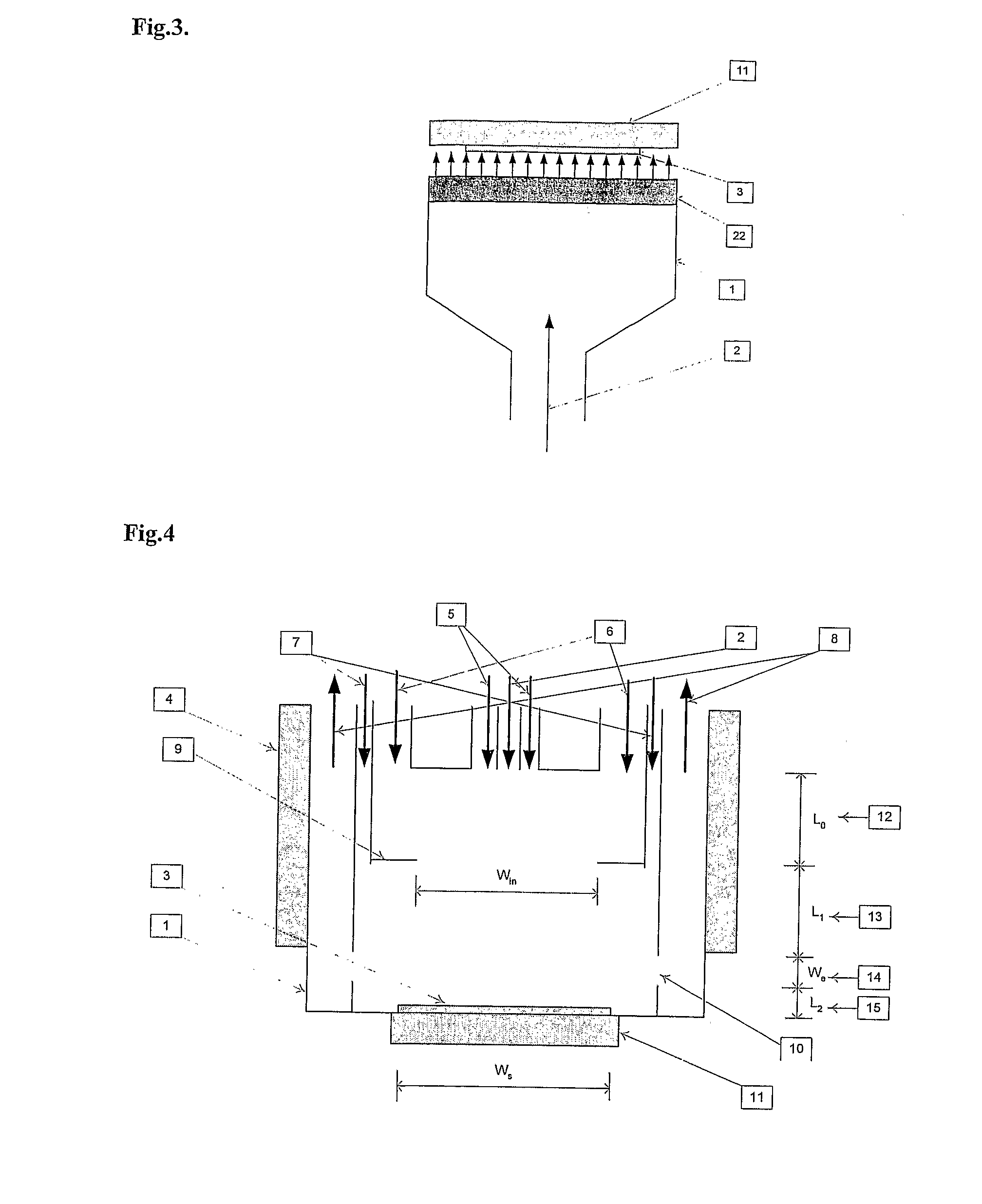
[0064]A c-plane-oriented sapphire substrate of About 2 inches in diameter is loaded on to the substrate holder of a HVPE vertical reactor according to FIG. 4, 6, 7 or 8. The sapphire is deposited with MOCVD grown GaN of 2 μm thickness, and the sapphire is mechanically thinned and weakened.

[0065]The gas heater is heated to a temperature of about 500° C. N2 is introduced through all gas injectors 2, 5, 6 and 7 for about 30 minutes to purge the tube assembly of air. The pressure of the growth chamber is maintained at 1 atm. Substrates are heated to a temperature of about 350° C. NH3 flow at about 1000 sccm is introduced into the chamber. The external GaCl gas precursor is produced by passing 10% Cl2 in N2 through a Ga bubbler, the gas transport line being made of nylon with a heating wire to maintain the nylon tube temperature around 125° C. The conversion rate is nearly 100% for GaCl. Then the substrates are heated to a temperature of about 1050° C.

[0066]Gas delivery to the growth cha...

example 2

[0070]The growth processes are similar to Example 1 in the case of a vertical HVPE reactor shown in FIG. 5 or 9, except the gas precursor of GaCl is produced in situ up-stream in the growth chamber. It is recommended that NH3 is switched on when the gases and substrates are heated above 500° C.

example 3

[0071]The growth processes are similar to Example 1, but the time-modulated growth method is modified. The growth is divided into etch, annealing, enhanced lateral growth and normal growth. In this example, the flow of reagent gases is etch (GaCl off, NH3 and HCl on with a gas flow of 80 sccm), annealing (GaCl off, NH3 and HCl on with a gas flow of 5 sccm), enhanced lateral growth (GaCl and NH3 on, HCl on with a gas flow of 5 sccm, total. H2 flow increasing from 60 to 200 scorn) and normal growth (GaCl and NH3 on, HCl on with gas flow of 5 sccm, total H2 flow of 60 sccm). The time for the etch, annealing, enhanced lateral growth and normal growth period is set to be 1, 1, 3 and 2 minutes respectively.


PUM

PropertyMeasurementUnit
diameteraaaaaaaaaa
lengthaaaaaaaaaa
diametersaaaaaaaaaa

Abstract

Deposited layers are advantageously obtained by utilizing a specific hydride vapour phase epitaxy deposition procedure. In this procedure, a vertical growth cell structure with extended diffusion layer, a homogenising diaphragm, sidewall purging gases, anal independent gas and substrate heaters is used for the deposition of III-V and VI compound semiconductors. This gas flow is uniformly mixed through the extended diffusion layer and directed so that it contacts the full surface of the substrate to produce high quality and uniform films. Exemplary of such gas flow configurations are the positioning of a substrate at a distance from the gas outlets to allow the extended diffusion and a diaphragm placed in a short distance above the substrate to minimise the impact of the convection effect and to improve the uniformity. This symmetrical configuration allows easy scale up from a single wafer to multi-wafer system. This vertical configuration allows the quick switching between different reactive gas precursors so that time modulated growth and etch processes can be employed to further minimise the defects density of the deposited materials.

Description

BACKGROUND OF THE INVENTION[0001]1. Field of the Invention[0002]The present invention relates to material deposition. More particularly, the invention relates to material hydride vapour phase epitaxy (HVPE) deposition using a vertical growth cell with extended diffusion and time modulated growth processes for growth of semiconductors of IV and III-V groups and their alloys.[0003]2. Description of the Prior Art[0004]Many processes have been developed for the deposition of materials, e.g. semiconductor materials, on a substrate. One such process involves the use of a precursor gas, i.e. a gas that upon contact with the substrate undergoes a modification such as a chemical reaction to yield a deposited layer. In these vapour deposition processes, generally, the gas flow and its spatial relationship to the substrate are carefully controlled. For example, in the most common spatial configuration employed in chemical vapour deposition (CVD) or hydride vapour phase epitaxy (HVPE), as shown...

Claims


Application Information

Patent Timeline
Patent Type & Authority Applications(United States)
IPC IPC(8): H01L21/20C23C16/30C23C16/44C30B25/02C30B25/14
CPCC23C16/303C23C16/4412C30B25/14C23C16/4557C30B25/02C23C16/45523H01L21/205H01L21/20
Inventor WANG, WANG NANGSTEPANOV, SERGEY IGOREVICH
Owner QUANTUM NIL LTD
Why Eureka
Try Eureka