Long wavelength vertical cavity surface emitting laser device and method of fabricating the same

a laser device and laser technology, applied in the direction of lasers, lasers using scattering effects, semiconductor lasers, etc., can solve the problems of weak coupling efficiency, difficult long-distance optical communication, gain and stability of gain medium can deteriorate, etc., to achieve low thermal conductivity, stable connection, and high reliability

Active Publication Date: 2008-06-12
ELECTRONICS & TELECOMM RES INST
View PDF8 Cites 22 Cited by
  • Summary
  • Abstract
  • Description
  • Claims
  • Application Information

AI Technical Summary

Benefits of technology

[0016]The present invention provides a surface emitting device which has an advantage of increased productivity due to the use of vertical cavity surface emitting laser (VCSEL) devices and is effective at releasing generated heat and a method of manufacturing the surface emitting laser device.
[0035]According to the present invention, problems of the conventional art can be overcome. These problems are as follows. A conventional surface emitting device is technologically complicated. For example, when a mirror layer material and an active layer material are separately grown, and then wafers are wafer-bonded in a following operation, or the wafers are metamorphically grown, and then a dielectric mirror layer is coupled to the wafers, reliability may deteriorate due to crystal defects or plastic deformation. The present invention can overcome these problems.
[0036]The present invention can realize a long wavelength vertical cavity surface emitting laser as a lattice matched crystal growth structure having high reliability and ability to overcome the limitation of the material forming the conventional surface emitting device having a low thermal conductivity.
[0037]According to the present invention, a device is fabricated so that a stable connection is achieved between layers including the same kind of materials, instead of a connection between layers including different kinds of materials in order to improve thermal properties. An aperture region of an air layer is formed on a heating portion, and then a dielectric layer having high thermal conductivity and a metal layer are deposited on the aperture region, and thus a laser can be easily used to emit heat, and operational properties and reliability can be improved.

Problems solved by technology

Surface emitting laser devices emit a beam in a direction perpendicular from a top surface of a substrate, unlike edge emitting laser devices emitting asymmetrically shaped beams and having weak coupling efficiency with respect to optical fibers.
However, since VCSEL devices for emitting light having wavelengths in the range of 850 to 980 nm have limits with respect to a distance and velocity at which light moves through an optical fiber, these VCSEL devices are used only for local area communication, and are difficult to be used in long-distance optical communication.
However, as nitrogen increases or the wavelength of oscillating light increases, the gain and stability of the gain medium can deteriorate, and it is difficult to obtain gain properties of a long wavelength in the range of 1.3 μm or more.
In the case of surface emitting layer devices including an InP substrate, it is difficult to obtain a pair of materials constituting a reflective mirror, which have a large difference between their refractive indexes.
In addition, since quaternary materials such as InGaAsP and InAlGaAs, which are used as materials for active layers or reflective mirrors, have low thermal conductivity corresponding to 0.1 times that of a binary material such as GaAs, the heat releasing properties of a device may deteriorate.
In long wavelength VCSEL devices, a unique small band gap of a material results in a remarkable decrease in the performance of a device and an increase in the temperature.
Therefore, erroneous wafer bonding may occur, the reliability and mass-productivity may be reduced, and costs may increase.
Fabrication processes can be simplified by using the monolithic method, but heat release properties can deteriorate due to the fact that it is difficult to grow a thick mirror layer and quaternary materials are used.

Method used


Image

  • Long wavelength vertical cavity surface emitting laser device and method of fabricating the same
  • Long wavelength vertical cavity surface emitting laser device and method of fabricating the same
  • Long wavelength vertical cavity surface emitting laser device and method of fabricating the same

Examples


Embodiment Construction

[0041]The present invention will now be described more fully with reference to the accompanying drawings, in which exemplary embodiments of the invention are shown. The invention may, however, be embodied in many different forms and should not be construed as being limited to the embodiments set forth herein; rather, these embodiments are provided so that this disclosure will be thorough and complete, and will fully convey the concept of the invention to those of ordinary skill in the art.

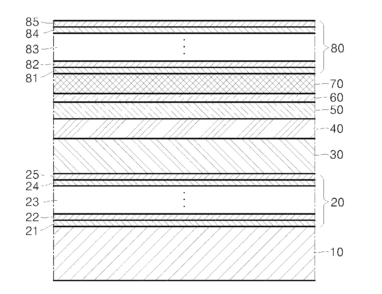
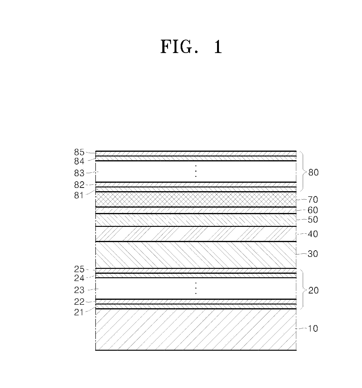
[0042]FIGS. 1 through 5 are cross-sectional views of a surface emitting layer device and are for explaining a method of fabricating the surface emitting layer device, according to embodiments of the present invention.

[0043]Referring to FIG. 1, a lower mirror layer 20, an active layer 40, a tunnel junction layer 60 and an upper mirror layer 80 are sequentially grown on a compound semiconductor substrate 10 by using an epitaxial growth method. At this time, a first conducting layer 30 may be further ...


PUM


Abstract

Provided is a vertical cavity surface emitting device. The surface emitting device includes a lower mirror layer emitting light having a long wavelength, an active layer providing an optical gain, a tunnel junction layer for confining a current, and an upper mirror layer, which are sequentially stacked on a compound semiconductor substrate, wherein a heat release layer is formed on side surfaces of at least one of the active layer, the tunnel junction layer and the upper mirror layer by using etching process, and the heat release layer has greater thermal conductivity than at least one of the active layer, the tunnel junction layer and the upper mirror layer.

Description

CROSS-REFERENCE TO RELATED PATENT APPLICATION[0001]This application claims the benefit of Korean Patent Application No. 10-2006-0123410, filed on Dec. 6, 2006 and Korean Patent Application No. 10-2007-0047284, filed on May 15, 2007 in the Korean Intellectual Property Office, the disclosures of which are incorporated herein in their entirety by reference.BACKGROUND OF THE INVENTION[0002]1. Field of the Invention[0003]The present invention relates to a surface emitting laser device and a method of fabricating the surface emitting laser device, and more particularly, to a long wavelength vertical cavity surface emitting laser device for optical communication, which has a band in the range of 1.3 to 1.6 μm, and a method of fabricating the long wavelength vertical cavity surface emitting laser device.[0004]This work was supported by the IT R&D program of MIC / IITA. [2005-S-051-02, Photonic device integrated module for optical access network][0005]2. Description of the Related Art[0006]Sur...

Claims


Application Information

Patent Timeline
Patent Type & Authority Applications(United States)
IPC IPC(8): H01S5/00
CPCB82Y20/00H01S5/024H01S5/02461H01S5/18308H01S2301/18H01S5/18313H01S5/18333H01S5/3095H01S5/34306H01S5/18311
Inventor PARK, MI-RANKWON, O-KYUN
Owner ELECTRONICS & TELECOMM RES INST
Why Eureka
Try Eureka