Solid-state imaging device and electronic device

a solid-state imaging and electronic device technology, applied in the direction of diodes, semiconductor devices, radiation controlled devices, etc., can solve the problems of difficult to modify the common conditions of pixel transistors and peripheral transistors, difficult to modify the specific dimensions of elements, and difficult to modify the conditions of forming peripheral transistors. , to achieve the effect of reducing the size of the floating diffusion portion, reducing the depletion layer, and increasing the siz

Active Publication Date: 2008-06-19
SONY SEMICON SOLUTIONS CORP
View PDF12 Cites 92 Cited by
  • Summary
  • Abstract
  • Description
  • Claims
  • Application Information

AI Technical Summary

Benefits of technology

[0033]In the method of producing the solid-state imaging device of the present invention, by forming in the floating diffusion portion formation region, the second second-conductivity-type semiconductor well region with the impurity concentration lower than the impurity concentration of the third second-conductivity-type semiconductor well region of the transistor portion formation region, and forming the first-conductivity-type diffusion region that forms the floating diffusion portion in the second second-conductivity-type semiconductor well region, the growth of the depletion layer in the floating diffusion portion is increased, and the parasitic capacitance in the floating diffusion portion can be decreased.
[0034]A solid-state imaging device according to an embodiment of the present invention may be reduced in size while suppressing a reduction in conversion efficiency due to an increase in volume of a floating diffusio

Problems solved by technology

Further, specifications (such as materials and dimensions) of elements are often limited by the level of manufacturing technology in a particular era (so-called process generation).
Therefore, it may be difficult to modify conditions for forming peripheral transistors even when an optical size is reduced.
Accordingly, in the manufacture of a small and lightweight solid-state imaging device under the present circumstances, it may be difficult to modify common conditions for pixel transistors and peripheral transi

Method used


Image

  • Solid-state imaging device and electronic device
  • Solid-state imaging device and electronic device
  • Solid-state imaging device and electronic device

Examples


examples

[0094]Examples of the present invention will be described.

[0095]A first example of the present invention will be described with reference to FIGS. 21A to 21C.

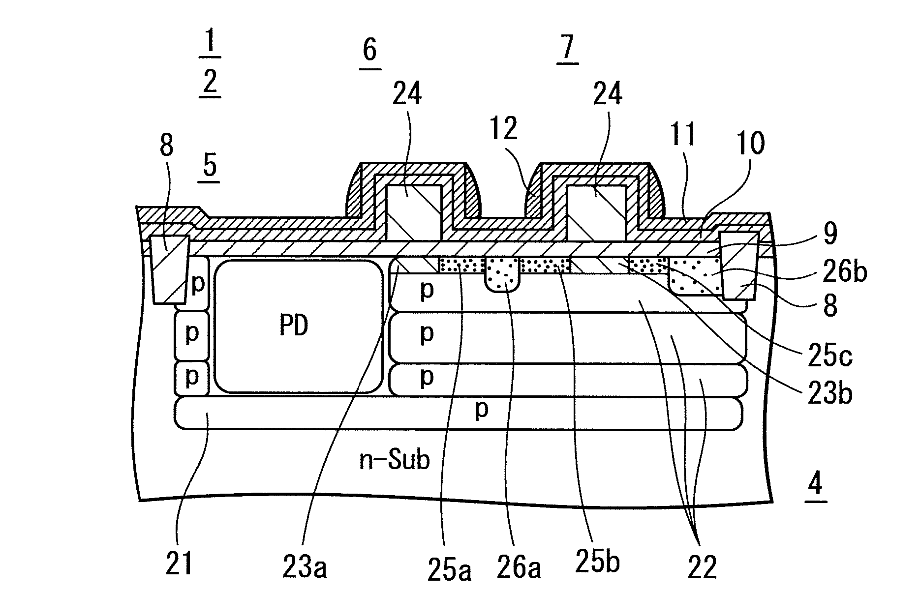
[0096]In the solid-state imaging device 1 of the present example, an impurity concentration in the FD, specifically, the extension implantation region 25a of the pixel 2 is lower than an impurity concentration in an impurity diffusion layer of a transistor of the peripheral circuit 3. Impurities are generally implanted in the extension implantation region 25a at a surface impurity concentration of 1×10²⁰ / cm3 or more due to the presence of the impurity diffusion layer in the transistor of the peripheral circuit 3. However, in the solid-state imaging device 1 of the present example, an impurity concentration in the extension implantation region 25a is as low as one-tenth to one-hundredth of such a surface impurity concentration.

[0097]Image quality may be preferentially improved in this configuration, since contact resistance usua...


PUM


Abstract

There is provided a solid-state imaging device including an imaging region having a plurality of pixels arranged in a two-dimensional matrix and a peripheral circuit detecting output signals from the pixels. An impurity concentration in a transistor of each pixel is lower than an impurity concentration in a transistor of the peripheral circuit. Further, the impurity concentration of a semiconductor well region under a floating diffusion portion in the pixel is set to be lower than the impurity concentration of a semiconductor well region under a transistor portion at the subsequent stage of the floating diffusion portion.

Description

CROSS REFERENCES TO RELATED APPLICATIONS[0001]The present invention contains subject matter related to Japanese Patent Applications JP 2006-273254 and JP 2006-290382 filed in the Japanese Patent Office on Oct. 4, 2006 and Oct. 25, 2006, respectively, the entire contents of which being incorporated herein by reference.BACKGROUND OF THE INVENTION[0002]1. Field of the Invention[0003]The present invention relates to a solid-state imaging device and an electronic device including the solid-state imaging device.[0004]2. Description of the Related Art[0005]CMOS (Complementary Metal-Oxide-Semiconductor) solid-state imaging devices (CMOS image sensors) are solid-state imaging devices particularly attracting attention in recent years. Such a CMOS solid-state imaging device includes an imaging region having many pixels arranged in a two-dimensional matrix; and a peripheral circuit provided around the imaging region. In the imaging region, each of the pixels has a floating diffusion (FD) layer ...

Claims


Application Information

Patent Timeline
IPC IPC(8): H01L27/146H01L31/18
CPCH01L27/14609H01L27/14689H01L27/14643H01L27/146
Inventor SATO, MAKIOOKI, SUSUMU
Owner SONY SEMICON SOLUTIONS CORP
Why Eureka
Try Eureka