Apparatus for inspecting defects

a technology of defects and apparatus, applied in the field of apparatus and methods for inspecting defects, can solve the problems of insufficient consideration for achieve the effects of improving the defect detection ratio, clearer view of defects present, and high sensitivity

Inactive Publication Date: 2008-06-19
HITACHI HIGH-TECH CORP
View PDF3 Cites 55 Cited by
  • Summary
  • Abstract
  • Description
  • Claims
  • Application Information

AI Technical Summary

Benefits of technology

[0005]An object of the present invention is to provide a defect inspection apparatus adapted to solve the above problem and to improve a defect detection ratio during defect inspection of a mixed-type wafer (such as system LSI) or the like by detecting defects with high sensitivity and detecting a wide variety of defect species.
[0006]In the present invention, a reflecting objective lens free from chromatic aberration is employed to suppress changes in brightness due to multi-wavelength illumination (i.e., illumination with the irradiation light having a plurality of wavelength bands), to provide a clearer view of defects present on a sample, by means of selective wavelength detection in order to improve sensitivity, and to allow one spatial image on the sample to be acquired as different kinds of optical images.
[0041]has, on at least either of the first and second detection optical paths, an ND filter for reducing the light in intensity; and

Problems solved by technology

In the above two citations (Documents 1 and 2), however, sufficient consideration has not been given to improving a defect detection ratio by, during defect inspection of a mixed-type wafer (such as system LSI) or other electronic components each inclusive of a memory block formed with a periodic circuit pattern, and of a logic circuit block formed with an irregular circuit pattern (non-periodic circuit pattern), detecting defects with high sensitivity and detecting a wide variety of defect species.

Method used


Image

  • Apparatus for inspecting defects
  • Apparatus for inspecting defects
  • Apparatus for inspecting defects

Examples


first embodiment

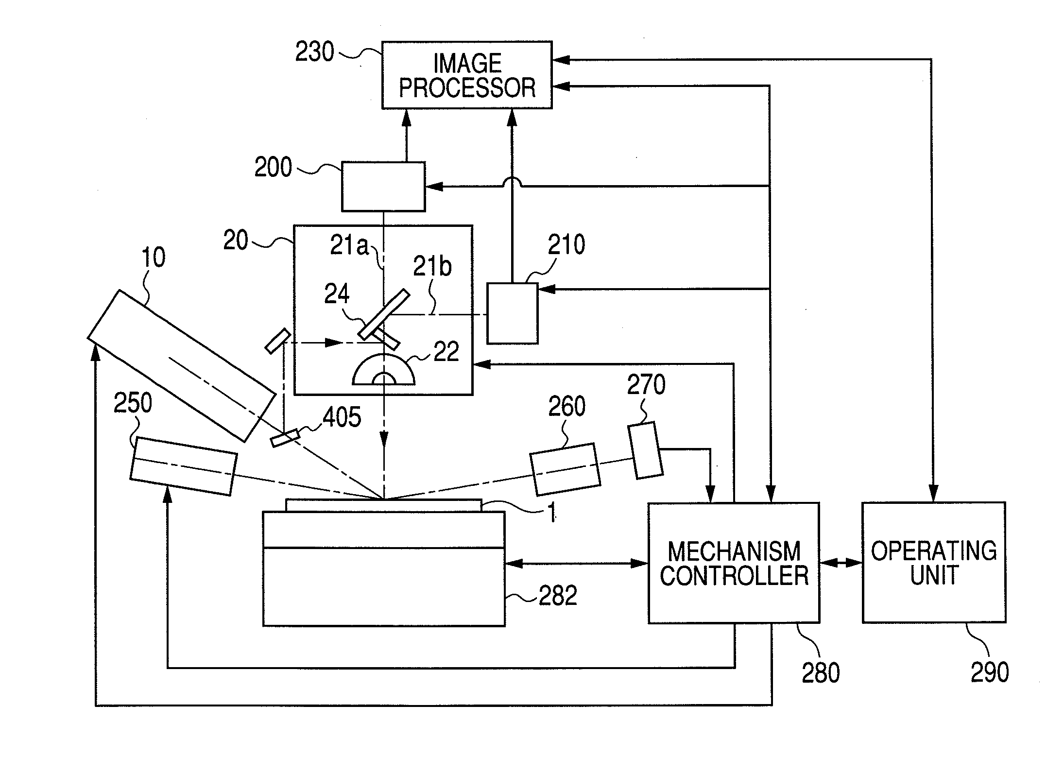
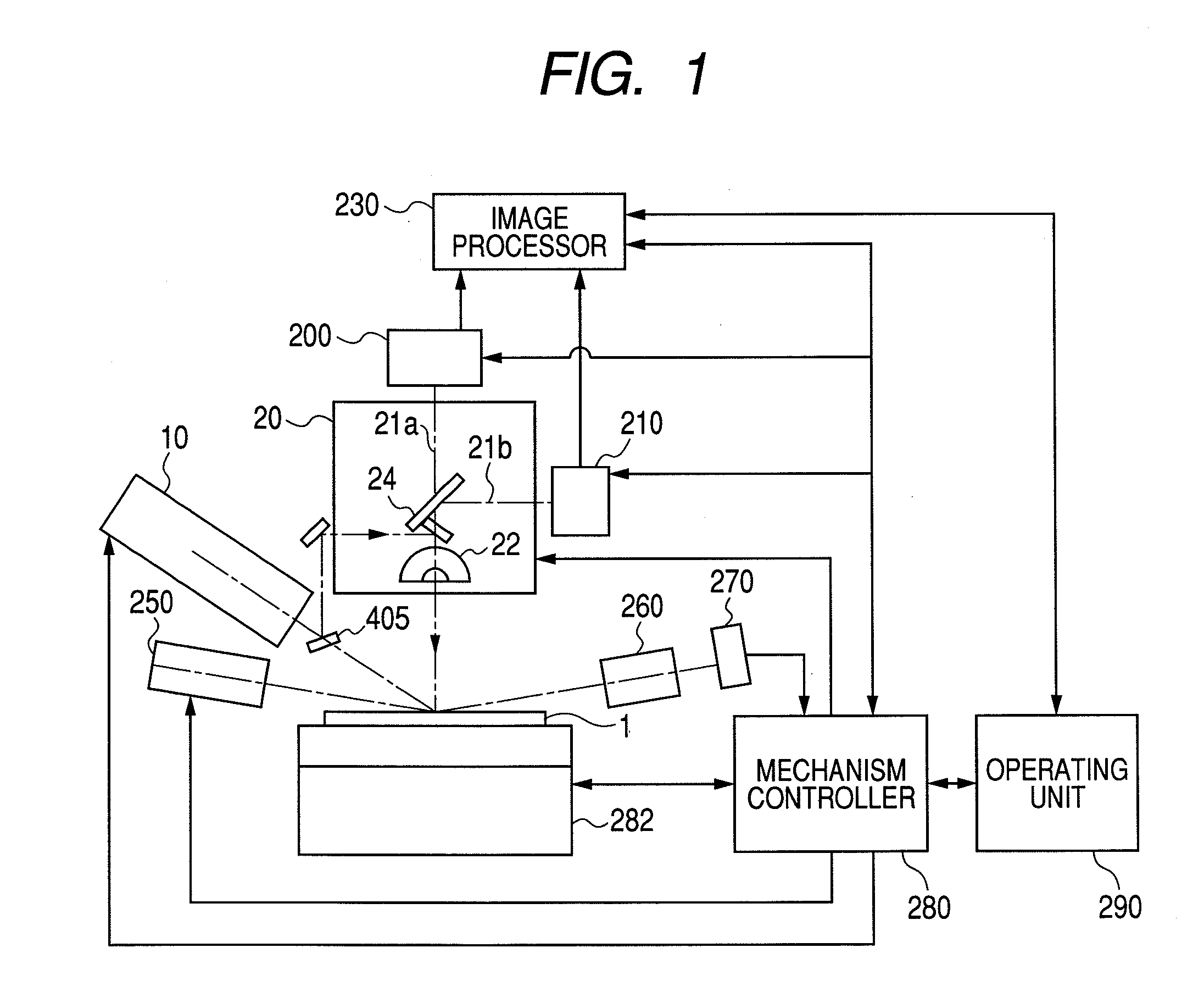
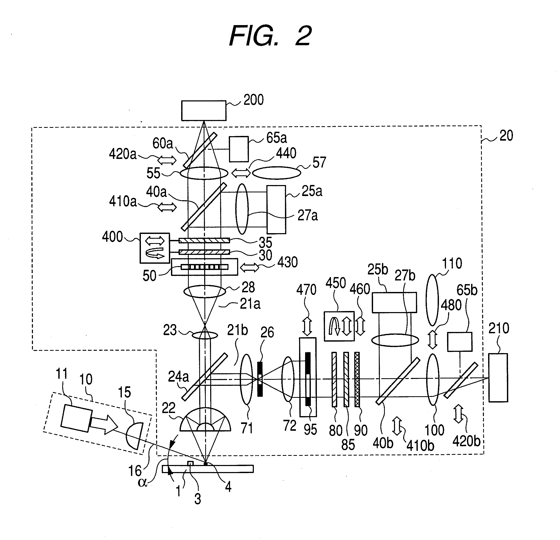
[0059]A schematic configuration of an optical defect inspection apparatus according to the present invention is shown in FIG. 1. A darkfield illumination optical system 10 conducts oblique darkfield illumination upon a wafer (sample) 1 from a normal direction thereof with illumination light of a plurality of wavelengths or a plurality of wavelength bands, through an exterior of a reflecting objective lens. A darkfield detection optical system 20 with a reflecting objective lens 22 free from chromatic aberration captures (converges) the light scattered from the defects or other foreign substances or patterns existing on the wafer (sample) 1. The darkfield detection optical system 20 has a beam splitter 24 to branch a detection optical path into a first detection optical path and a second detection optical path. The beam splitter 24 is either a dichroic mirror for wavelength separation, a polarized beam splitter for polarized beam separation, or a beam splitter for simple branching ba...


PUM

PropertyMeasurementUnit
field sizeaaaaaaaaaa
ArF wavelengthaaaaaaaaaa

Abstract

This invention is a defect inspection apparatus having a reflecting objective lens free from chromatic aberration, or an achromatic catadioptric lens, and a dioptric objective lens, and thus constructed to suppress changes in brightness due to multi-wavelength illumination (i.e., illumination with the irradiation light having a plurality of wavelength bands), to provide a clearer view of defects present on a sample, by means of selective wavelength detection in order to improve sensitivity, and to allow one spatial image on the sample to be acquired as different kinds of optical images.

Description

BACKGROUND OF THE INVENTION[0001]The present invention relates to an apparatus and method for inspecting defects, contamination, and other foreign substances present on minute patterns formed on a substrate through a thin-film process represented by a semiconductor manufacturing process and a flat-panel display manufacturing process.[0002]A conventional apparatus for inspecting defects in semiconductors is disclosed in, for example, International Patent Publication WO2003 / 0069263. The conventional inspection apparatus described in WO2003 / 0069263 illuminates the surface of a wafer obliquely with laser light, and after the light has been scattered from the wafer surface, captures the scattered light by use of an objective lens disposed above the wafer. The scattered light that has been captured is detected according to the particular scattering angle by a plurality of detectors. Detection images that have thus been obtained are compared with images of adjacent dies in order to detect ...

Claims


Application Information

Patent Timeline
Patent Type & Authority Applications(United States)
IPC IPC(8): G01N21/88
CPCG01N21/21G01N21/4788G01N21/94G01N2021/9513G01N21/95623G01N2021/8822G01N21/9501
Inventor SHIBATA, YUKIHIROMAEDA, SHUNJI
Owner HITACHI HIGH-TECH CORP
Why Eureka
Try Eureka