Chemical mechanical polishing pad

Active Publication Date: 2008-06-26
ROHM & HAAS ELECTRONICS MATERIALS CMP HLDG INC
View PDF31 Cites 20 Cited by
  • Summary
  • Abstract
  • Description
  • Claims
  • Application Information

AI Technical Summary

Benefits of technology

[0006]One aspect of the invention provides a chemical mechanical polishing pad suitable for polishing at least one of semiconductor, optical and magnetic substrates, the polishing pad having a high modulus component forming a continuous polymeric matrix and an impact modifier within the continuous polymeric matrix, the high modulus component having a modulus of at least 100 M

Problems solved by technology

The fabrication of these semiconductor devices continues to become more complex due to requirements for devices with higher operating speeds, lower leakage currents and reduced power consumption.
The devices' smaller scale and increased complexity have led to greater demands on CMP consumables, such as polishing pads and polishing solutions.
In addition, as integrated circuits' feature sizes decrease, CMP-induced defectivity, such as, scratching becomes a greate

Method used


Image

  • Chemical mechanical polishing pad
  • Chemical mechanical polishing pad
  • Chemical mechanical polishing pad

Examples


Embodiment Construction

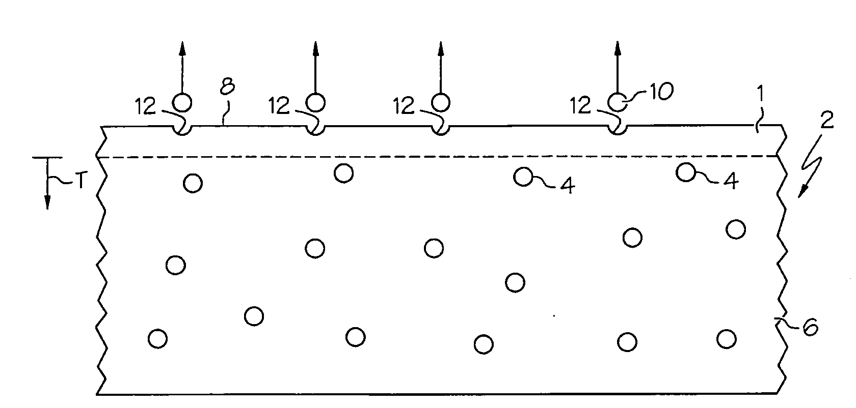
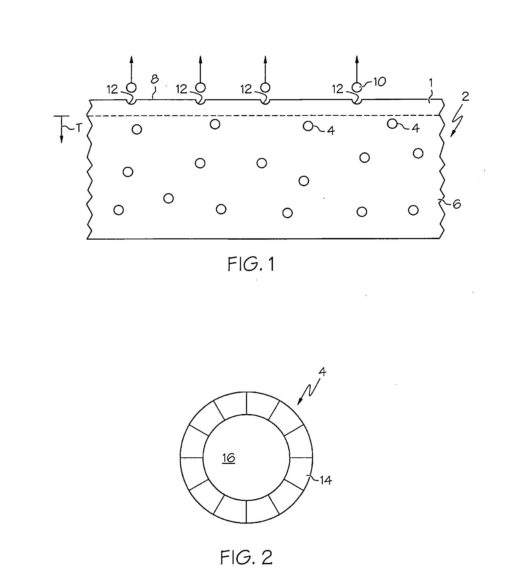
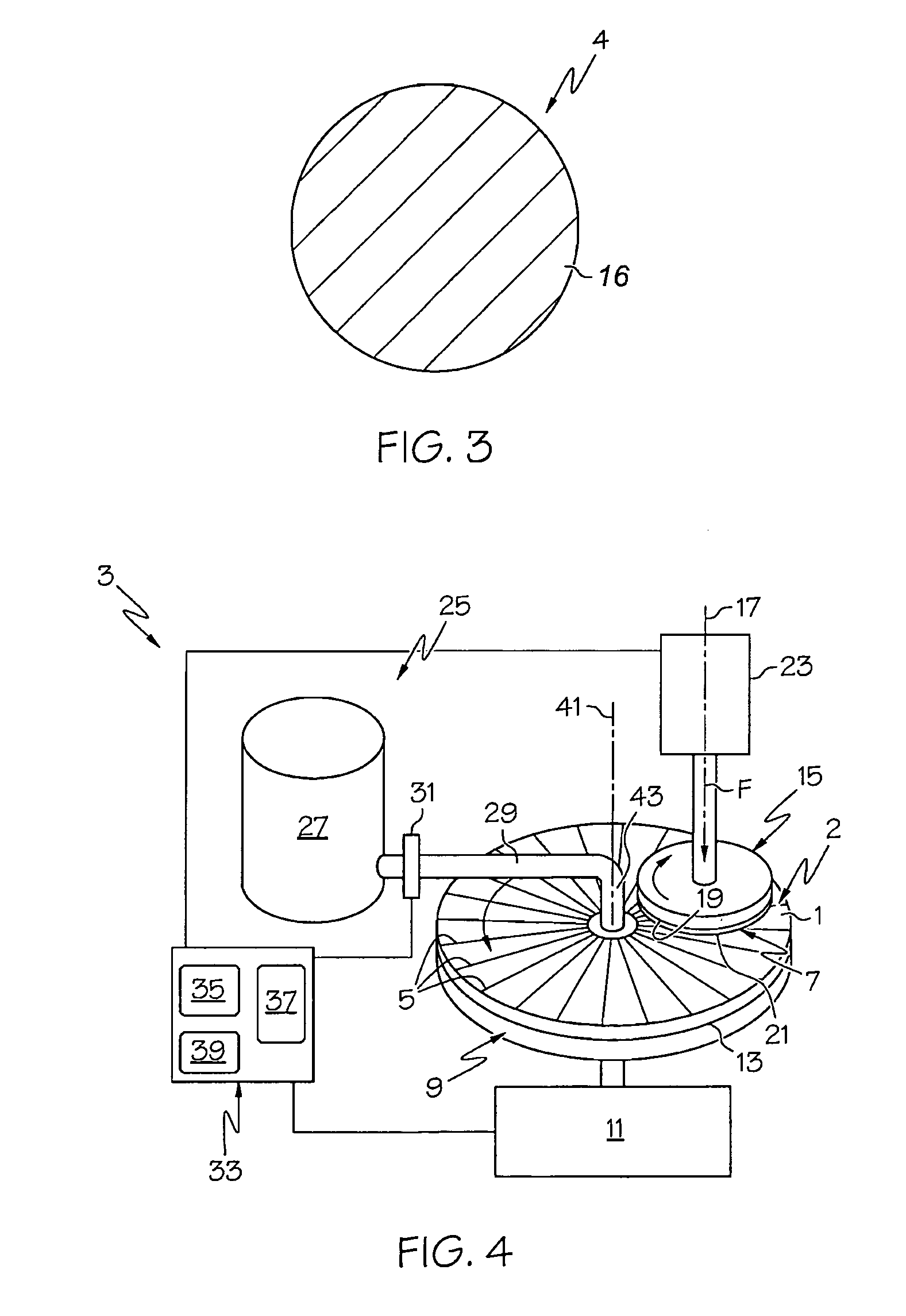
[0012]The invention provides a polishing pad suitable for planarizing at least one of semiconductor, optical and magnetic substrates, the polishing pad comprising a polymeric matrix. For example, the polishing pads may be suitable for polishing and planarizing several semiconductor wafer applications, such as STI (HDP / SiN, TEOS / SiN or SACVD / SiN), copper, barrier (Ta, TaN, Ru) and tungsten. In addition, these pads maintain their surface structure to facilitate eCMP (“electrochemical mechanical planarization”) applications. For example, perforations through the pad, the introduction of conductive-lined grooves or the incorporation of a conductor, such as a conductive fiber or metal wire, can transform the pads into eCMP polishing pads. The polishing pad's structure improves the pad's impact resistance and can have an unexpected benefit in polishing performance, such as planarization and defectivity. For purposes of this invention, an increase in a polishing pad's impact resistance may...


PUM

PropertyMeasurementUnit
Pressureaaaaaaaaaa
Pressureaaaaaaaaaa
Pressureaaaaaaaaaa

Abstract

A chemical mechanical polishing pad is suitable for polishing at least one of semiconductor, optical and magnetic substrates. The polishing pad has a high modulus component forming a continuous polymeric matrix and an impact modifier within the continuous polymeric matrix. The high modulus component has a modulus of at least 100 MPa. The impact modifier includes a low modulus component having a modulus of at least one order of magnitude less than the high modulus component that increases the impact resistance of the polishing pad.

Description

BACKGROUND OF THE INVENTION[0001]This specification relates to polishing pads useful for polishing and planarizing substrates, such as semiconductor substrates or magnetic disks.[0002]Polymeric polishing pads, such as polyurethane, polyamide, polybutadiene and polyolefin polishing pads represent commercially available materials for substrate planarization in the rapidly evolving electronics industry. Electronics industry substrates requiring planarization include silicon wafers, patterned wafers, flat panel displays and magnetic storage disks. In addition to planarization, it is essential that the polishing pad not introduce excessive numbers of defects, such as scratches or other wafer non-uniformities. Furthermore, the continued advancement of the electronics industry is placing greater demands on the planarization and defectivity capabilities of polishing pads.[0003]For example, the production of semiconductors typically involves several chemical mechanical planarization (CMP) pr...

Claims


Application Information

Patent Timeline
IPC IPC(8): B24B1/00B24D99/00
CPCB24D3/26B24B37/24B24B37/11B24D13/14H01L21/304
Inventor KULP, MARY JOJAMES, DAVID B.ANTRIM, ROBERT F.
Owner ROHM & HAAS ELECTRONICS MATERIALS CMP HLDG INC
Why Eureka
Try Eureka