CRYSTAL GROWTH OF M-PLANE AND SEMIPOLAR PLANES OF (Al, In, Ga, B)N ON VARIOUS SUBSTRATES

a technology of m-plane and semi-polar planes, which is applied in the direction of crystal growth process, polycrystalline material growth, chemically reactive gas, etc., can solve the problems of localized stacking faults in the edges of window regions, and achieves less leakage current, less polarization fields, and longer lifetimes

Inactive Publication Date: 2008-07-10
JAPAN SCI & TECH CORP
View PDF55 Cites 46 Cited by
  • Summary
  • Abstract
  • Description
  • Claims
  • Application Information

AI Technical Summary

Benefits of technology

[0051]The present invention also takes advantage of the orientation of non-polar III-Nitrides to eliminate polarization fields. As a result, with the material produced by utilizing this invention, device improvements such as longer lifetimes, less leakage c...

Problems solved by technology

Also, stacking faults was locali...

Method used


Image

  • CRYSTAL GROWTH OF M-PLANE AND SEMIPOLAR PLANES OF (Al, In, Ga, B)N ON VARIOUS SUBSTRATES
  • CRYSTAL GROWTH OF M-PLANE AND SEMIPOLAR PLANES OF (Al, In, Ga, B)N ON VARIOUS SUBSTRATES
  • CRYSTAL GROWTH OF M-PLANE AND SEMIPOLAR PLANES OF (Al, In, Ga, B)N ON VARIOUS SUBSTRATES

Examples


Embodiment Construction

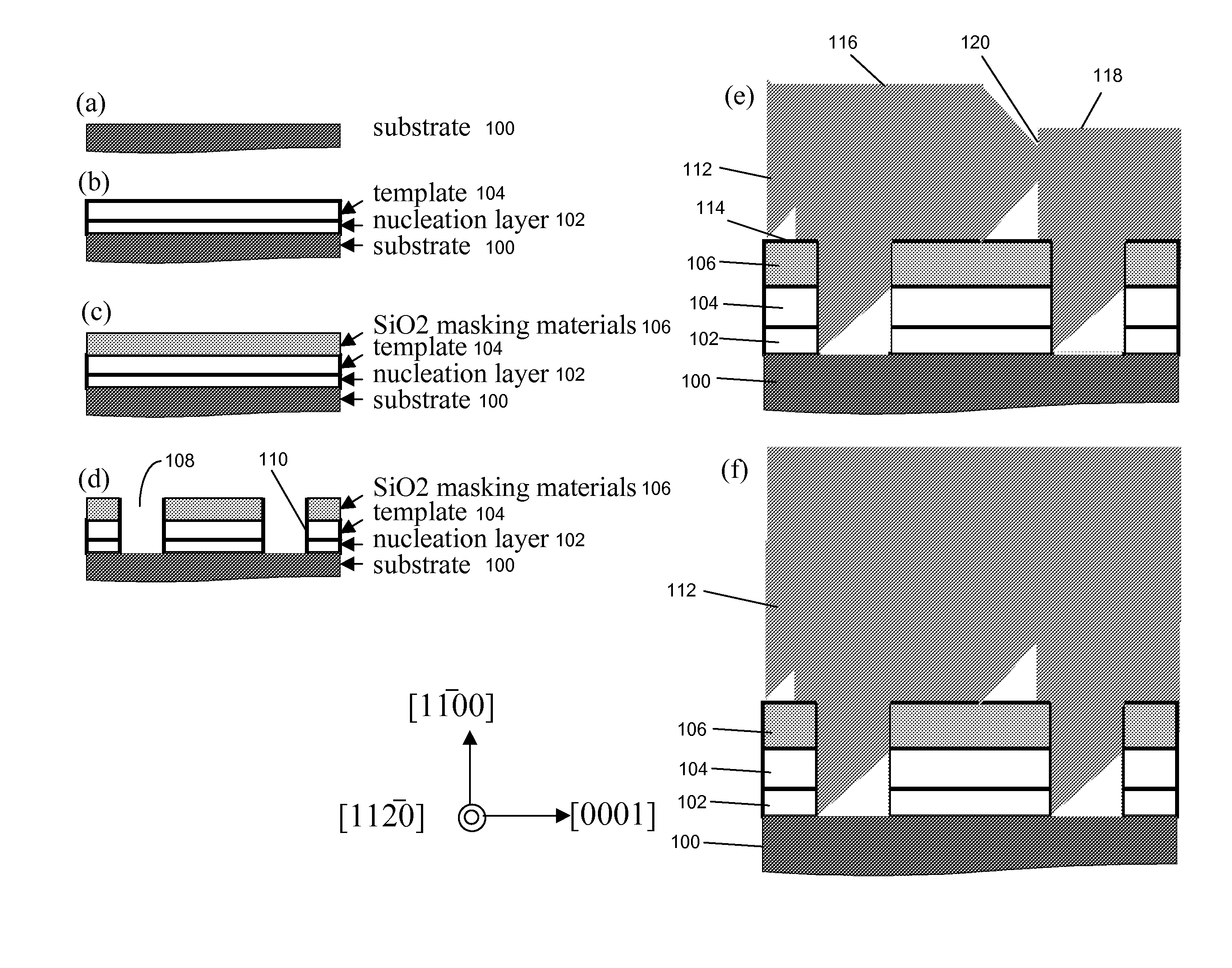
[0060]In the following description of the preferred embodiment, reference is made to the accompanying drawings that form a part hereof, and in which is shown by way of illustration a specific embodiment in which the invention may be practiced. It is to be understood that other embodiments may be utilized and structural changes may be made without departing from the scope of the present invention.

Overview

[0061]Conventional growth technique of GaN materials has two problems because growth direction of GaN is polar c-direction, and uses heteroepitaxy, which causes higher defects density.

[0062]Growth GaN along c-direction is relatively easy; however, this [0001] c-direction cause lower performance in optical devices due to polarized fields causing electrons and holes charge separation in the active regions. To eliminate this effect, growth on non-polar plane is suggested. Between a-plane and m-plane, m-plane is promising, because m-plane has stronger stability and higher Indium incorpor...


PUM


Abstract

A method of reducing threading dislocation densities in non-polar such as a- {11-20} plane and m-{1-100} plane or semi-polar such as {10-1n} plane III-Nitrides by employing lateral epitaxial overgrowth from sidewalls of etched template material through a patterned mask. The method includes depositing a patterned mask on a template material such as a non-polar or semi polar GaN template, etching the template material down to various depths through openings in the mask, and growing non-polar or semi-polar III-Nitride by coalescing laterally from the tops of the sidewalls before the vertically growing material from the trench bottoms reaches the tops of the sidewalls. The coalesced features grow through the openings of the mask, and grow laterally over the dielectric mask until a fully coalesced continuous film is achieved.

Description

[0001]This application claims the benefit under 35 U.S.C. Section 119(e) of co-pending and commonly-assigned U.S. provisional patent application, Ser. No. 60 / 869,701, filed Dec. 12, 2006, entitled “CRYSTAL GROWTH OF M-PLANE AND SEMI-POLAR PLANES OF (Al, In, Ga, B)N ON VARIOUS SUBSTRATES,” by Kwang C. Kim et al., which application is incorporated by reference herein.[0002]This application is related to the following co-pending and commonly-assigned applications:[0003]U.S. Utility application Ser. No. 10 / 581,940, filed on Jun. 7, 2006, by Tetsuo Fujii, Yan Gao, Evelyn. L. Hu, and Shuji Nakamura, entitled “HIGHLY EFFICIENT GALLIUM NITRIDE BASED LIGHT EMITTING DIODES VIA SURFACE ROUGHENING,” attorney's docket number 30794.108-US-WO (2004-063), which application claims the benefit under 35 U.S.C Section 365(c) of PCT Application Ser. No. US2003 / 03921, filed on Dec. 9, 2003, by Tetsuo Fujii, Yan Gao, Evelyn L. Hu, and Shuji Nakamura, entitled “HIGHLY EFFICIENT GALLIUM NITRIDE BASED LIGHT ...

Claims


Application Information

Patent Timeline
IPC IPC(8): C30B23/04H01L33/00
CPCH01L21/0254H01L21/02609H01L21/02636H01L21/02639H01L21/02647H01L21/02458H01L33/007C30B25/04C30B29/403H01L21/02378H01L21/0265
Inventor KIM, KWANG CHOONGSCHMIDT, MATHEW C.WU, FENGHIRAI, ASAKOMCLAURIN, MELVIN B.DENBAARS, STEVEN P.NAKAMURA, SHUJISPECK, JAMES S.
Owner JAPAN SCI & TECH CORP
Why Eureka
Try Eureka