Ferroelectric Thin Films and Devices Comprising Thin Ferroelectric Films

a technology of ferroelectric films and ferroelectric thin films, which is applied in the direction of generators/motors, instruments, other domestic objects, etc., can solve the problems of limiting the fabrication process to very few cases, wdm optical communication systems are usually very expensive, and the thin films obtained by these methods, so as to reduce the size of optical devices and reduce the price of integrated systems.

Inactive Publication Date: 2008-07-10
ETH ZZURICH
View PDF12 Cites 30 Cited by
  • Summary
  • Abstract
  • Description
  • Claims
  • Application Information

AI Technical Summary

Benefits of technology

[0015]According to a preferred embodiment, prior to bonding the block to the second substrate, the first substrate is provided with a electrode layer prior to the bonding. This solves the additional problem of finding ways to apply voltages to such a thin ferroelectric crystal layer. In addition to the electrode layer, which may or may not be structured, a top electrode may be placed, so that the ferroelectric layer, including possible cladding layers, is sandwiched between two electrodes. This opens the possibility of specifically using electro-optic, piezoelectric, pyroelectric etc....

Problems solved by technology

Since different technologies and materials are used, the WDM optical communication systems are usually very expensive and require a large space.
However the thin films obtained by these methods have two main problems.
This will limit the fabrication process to very few cases and ...

Method used


Image

  • Ferroelectric Thin Films and Devices Comprising Thin Ferroelectric Films
  • Ferroelectric Thin Films and Devices Comprising Thin Ferroelectric Films
  • Ferroelectric Thin Films and Devices Comprising Thin Ferroelectric Films

Examples


Embodiment Construction

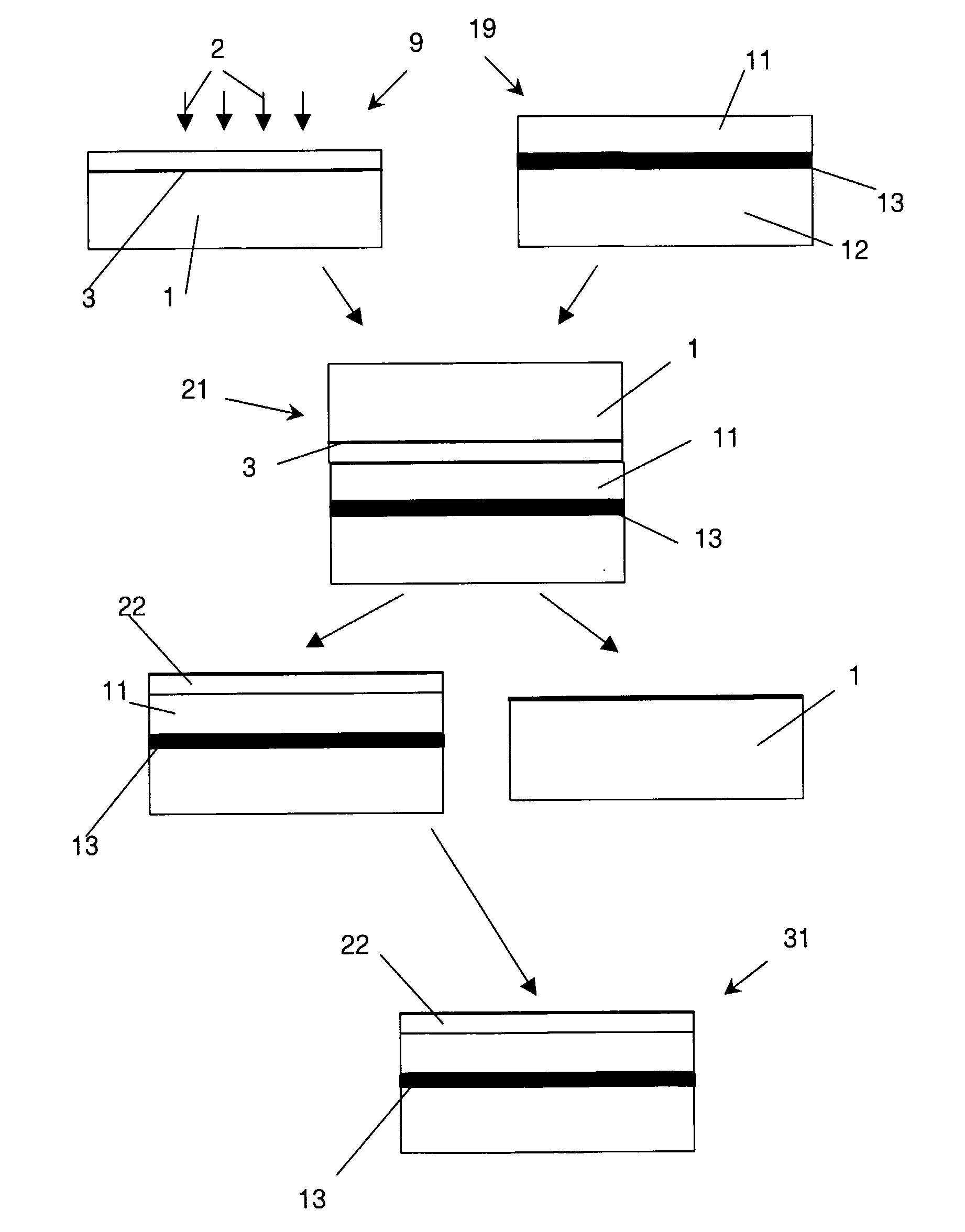
[0046]A first general embodiment of the present invention is shown in FIG. 1. This figure shows a basic procedure, which is used for the fabrication of thin films of nonlinear optical crystals. As is shown in FIG. 1, first a LiNbO3 ferroelectric crystal 1 is ion implanted using ionized He+ ions 2. The He+ ions are accelerated in an electric field and are used to bombard the ferroelectric crystal. The energy for these ions varies between 50 keV to 1 Mev. Because the He+ ions penetrate into the crystal, a damaged layer 3 is formed inside the crystal. In this layer the bonding between the adjacent atoms is broken due to the presence of the He atom.

[0047]The ferroelectric crystal in this embodiment as well as in other preferred embodiments is a bulk crystal (as opposed to grown layer films). Bulk crystals in this context are crystals that do not rely on a support (or growth) substrate and the size of which usually exceeds 100 μm in all three dimensions. Bulk crystals may be fabricated f...


PUM

PropertyMeasurementUnit
Fractionaaaaaaaaaa
Thicknessaaaaaaaaaa
Dispersion potentialaaaaaaaaaa

Abstract

A method of producing a device with a ferroelectric crystal thin film on a first substrate including the steps of providing a ferroelectric crystal, of irradiating a first surface of the ferroelectric crystal with ions so that a damaged layer is created underneath the first surface, of bonding a block of material including the first substrate to the ferroelectric crystal to create a bonded element, wherein an interface is formed between the first surface and a second surface of the block, and of heating the bonded element and separating it at the damaged layer, so that a ferroelectric crystal layer remains supported by the first substrate. By this method, very thin films—down to thicknesses of a fraction of a micrometer—of ferroelectric crystals may be fabricated without jeopardizing the monocrystalline structure.

Description

BACKGROUND OF THE INVENTION[0001]1. Field of the Invention[0002]The invention generally relates to applications of thin films of ferroelectric materials in integrated optical devices for telecommunication and data communication. The thin films of ferroelectric materials can also be used in applications such as electronic memory devices, pyroelectric detectors and piezoelectric actuators. In particular, the invention relates to fabrication of thin films of nonlinear optical materials, and to integrated optical devices for amplification and switching of light-wave signals.[0003]2. Description of Related Art[0004]Owing to large frequency-bandwidth of optical fibers, light-wave technology provides the ability to send a large amount of data using a very small fiber. To maximize the transmission capability of optical fibers, one has to use wavelength division multiplexing (WDM) technology. The current long-haul communication systems use WDM technology for transmitting large amounts of dat...

Claims


Application Information

Patent Timeline
IPC IPC(8): G11C11/22B29C65/00H01L41/00G02B6/10B29D11/00G02B6/12G02B6/34G02F1/035G02F1/355G02F1/377G02F1/39H01L21/20H01L21/316H01L21/762H01L37/02H01L41/22H01L41/312
CPCG02B6/12007G02B6/29355G02B6/29394G02F1/035G02F1/3551G02F1/377H01L41/22G11C11/22H01L21/2007H01L21/31691H01L21/76254H01L37/02G02F2001/392G02F1/392H01L21/02197H10N15/10H10N30/072
Inventor GUNTER, PETERRABIEI, PAYAM
Owner ETH ZZURICH
Why Eureka
Try Eureka