Sti of a semiconductor device and fabrication method thereof

a technology of semiconductor devices and fabrication methods, which is applied in the direction of semiconductor/solid-state device manufacturing, electrical equipment, basic electric elements, etc., can solve the problems of ozone-assisted sacvd, deposited sacvd film is apt to shrink, and conventional cvd methods have no longer provided satisfactory step coverage when dealing with high aspect ratio trenches, etc., to achieve low deposition sensitivity, good gap filling capacity, and convenient quality

Active Publication Date: 2008-07-10
UNITED MICROELECTRONICS CORP
View PDF5 Cites 37 Cited by
  • Summary
  • Abstract
  • Description
  • Claims
  • Application Information

AI Technical Summary

Benefits of technology

[0015]It is an advantage of the claimed invention that the reactant gas with a high O3 / TEOS flow ratio is employed to form a first silicon oxide layer so that the first silicon oxide layer have a preferable quality, such as with good gap fill capacity, low deposition sensitivity, and low shrinkage. As a result, the first silicon oxide layer formed in the trench is conformal, which can uniformly and completely fill a trench with a width smaller than 45 nanometers in a void-free manner. In addition, according to the present invention, a reactant gas with a less second O3 / TEOS flow ratio is provided to perform the second deposition process after the stop of the first deposition process, which forms the second silicon oxide layer with a higher rate to effectively fill large trenches. Therefore, the claimed invention can give consideration to the quality of STI with different sizes and to the production rate of mass fabrications.

Problems solved by technology

However, conventional CVD methods have no longer provided satisfactory step coverage when dealing with high aspect ratio trenches, such as the trenches with aspect ratios more than 6, which are typically encountered in the fabrication of advanced integrated circuits under 65 nm scale semiconductor fabrication process.
However, the prior art ozone-assisted SACVD techniques have several drawbacks when they are employed in the device isolation field.
First, after the high-temperature anneal treatment, the deposited SACVD film is apt to shrink.
Besides, the film quality of the SACVD silicon oxide and its resistance to wet etchant are not high enough.
Furthermore, the deposition sensitivity of the SACVD silicon oxide is not low enough.
Another problem encountered when employing SACVD to form trench isolation regions includes seams and voids occurring in the dielectric films in the trenches.
The seam defect 18 and void defect 20 are concerned because they cannot be removed by mere high-temperature nitrogen anneal as mentioned supra, and because they are subject to corrosion or attacks by the wet etchant used in the subsequent wet cleaning procedures, which affects the performance of the semiconductor elements and causes polysilicon circuit shorts.
However, when the width of a trench is less than 65 nanometers or even less than 45 nanometers, the above-mentioned seam defect and void defect problems still occur in the silicon oxide layer formed by the TEOS ramp-up SACVD method.

Method used


Image

  • Sti of a semiconductor device and fabrication method thereof
  • Sti of a semiconductor device and fabrication method thereof
  • Sti of a semiconductor device and fabrication method thereof

Examples


first embodiment

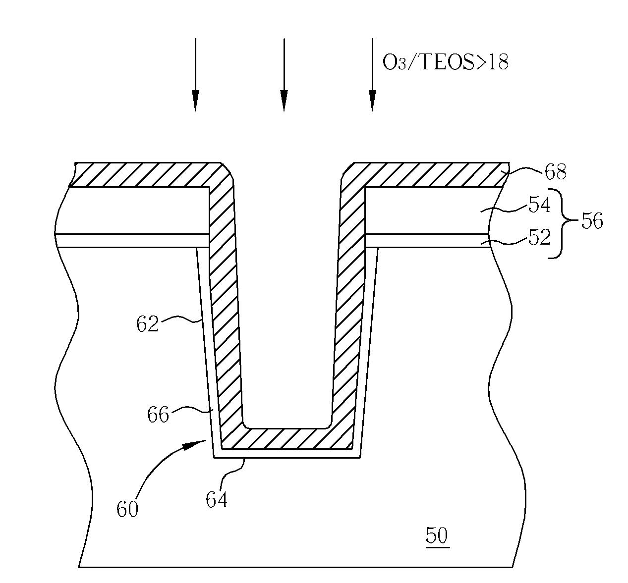
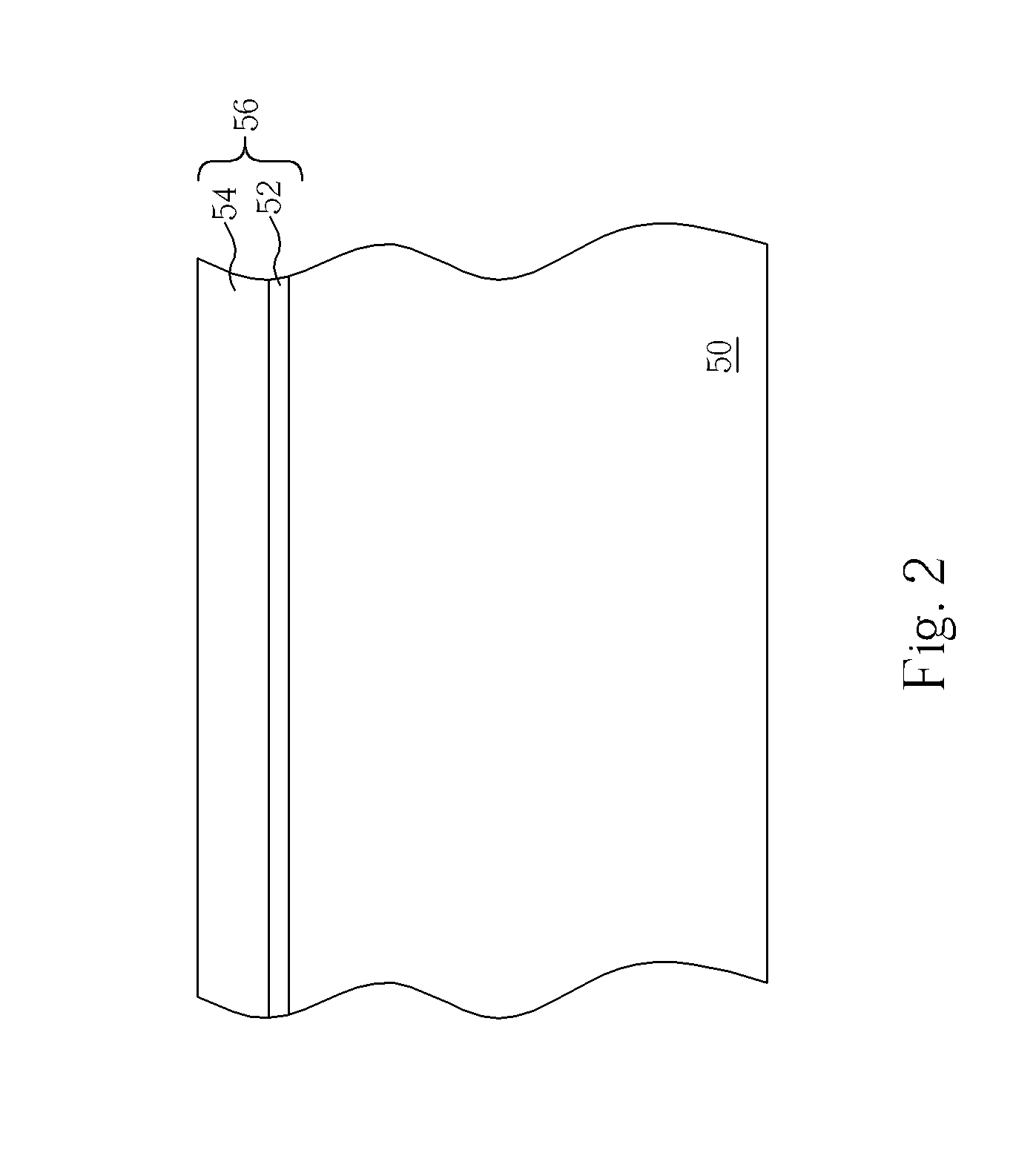
[0020]Please refer to FIGS. 2-6. FIGS. 2-6 are sectional schematic diagrams of a fabrication process of an STI according to the present invention. First, a semiconductor substrate 50, such as a silicon substrate, is provided, as shown in FIG. 2. Then, a pad oxide layer 52 is formed on the semiconductor substrate 50 with a thickness of about 30 angstroms to 200 angstroms, wherein the pad oxide layer 52 may be formed by a CVD process or a thermal oxidation process. After the formation of the pad oxide layer 52, a pad nitride layer 54 with a thickness of about 500 angstroms to 2000 angstroms is formed covering the pad oxide layer 52. The pad oxide layer 52 and the pad nitride layer 54 compose a mask layer 56.

[0021]As shown in FIG. 3, a photolithography process and an etching process are sequentially performed to form an opening 58 in the mask layer 56. Then, the mask layer 56 is taken as an etching mask during another etching process to remove a portion of the semiconductor substrate 5...

second embodiment

[0025]In a semiconductor wafer, sallow trench isolations for electrically isolating elements may have different sizes and aspect ratios according to the design of electric circuits. For shallow trenches with various aspect ratios, each deposition process may produce silicon oxide layers with various gap filling performances. Therefore, the present invention would introduce the method of forming silicon oxide layers into a plurality of shallow trenches with different aspect ratios at the same time for fabricating shallow trench isolations in a single semiconductor wafer with good performance.

[0026]Please refer to FIGS. 7-11. FIGS. 7-11 are sectional schematic diagrams of fabrication process of a semiconductor device 136 according to a second embodiment of the present invention. Referring to FIG. 7, the semiconductor device 136 comprises a semiconductor substrate 100. A pad oxide layer 102, a pad nitride layer 104, and electrical elements (not shown) are positioned on the surface of t...


PUM

PropertyMeasurementUnit
widthaaaaaaaaaa
aspect ratiosaaaaaaaaaa
pressureaaaaaaaaaa

Abstract

A method for filling silicon nitride materials into a trench includes providing a substrate having a plurality of trenches, performing a first deposition process to form a first silicon nitride layer in the trenches, and performing a second deposition process to form a second silicon nitride layer in the trenches. The reactant gas of the first deposition process has a first O3 / TEOS flow ratio larger than a second O3 / TEOS flow ratio of the reactant gas of the second deposition process.

Description

BACKGROUND OF THE INVENTION[0001]1. Field of the Invention[0002]The invention relates to a shallow trench isolation (STI) of a semiconductor device and fabrication method thereof, and more particularly, to an STI of a semiconductor material fabricated by a multi-step deposition method with non-TEOS ramp up process.[0003]2. Description of the Prior Art[0004]In semiconductor products, silicon oxide materials and silicon nitride materials are generally used to form isolation structures for isolating electric elements or devices. Conventional oxide dielectric layers or isolation structures are fabricated by localized oxidation isolation (LOCOS) methods or thin film deposition processes. For example, some gases such as silane (SiH4), tetra-ethyl-ortho-silicate (TEOS) and oxygen are used in a thin film deposition process to form a dielectric layer. The chemical reaction between the gases forms a thin film on the semiconductor wafer to provide electrical insulation between devices.[0005]In...

Claims


Application Information

Patent Timeline
Patent Type & Authority Applications(United States)
IPC IPC(8): H01L21/31
CPCH01L21/02164H01L21/022H01L21/02271H01L21/76224H01L21/02337H01L21/31612H01L21/02274
Inventor HSU, SHAO-TACHEN, NENG-KUOTSAI, TENG-CHUN
Owner UNITED MICROELECTRONICS CORP
Why Eureka
Try Eureka