Nonvolatile semiconductor memory element excellent in charge retention properties and process for producing the same

a semiconductor memory element and charge retention technology, applied in the direction of semiconductor devices, basic electric elements, electrical appliances, etc., can solve the problems of difficult formation of a thin film of insulators surrounding the floating gate of a flash memory, progress toward high performance, and difficulty in forming a thin film of insulators

Inactive Publication Date: 2008-07-17
ASAHI GLASS CO LTD +1
View PDF3 Cites 5 Cited by
  • Summary
  • Abstract
  • Description
  • Claims
  • Application Information

AI Technical Summary

Benefits of technology

[0045]According to the present invention, in a nonvolatile semiconductor memory element having a construction that a hardly oxidizable material composed of e.g. W, Ni or Co is used as an ultrafine particle floating gate or a single floating gate and an oxide such as SiO2 of an easily oxidizable material is used as an insulator encompassing the floating gate, wherein the ultrafine particle floating gate or a single floating gate is formed by using a physical forming method and the insulator is formed by using a physical forming method or a chemical forming method, it is possible to bond oxygen atoms with oxygen

Problems solved by technology

However, it is not easy to form a thin film of insulator surrounding a floating gate of a flash memory.
Thus, since forming of thin film of insulator is difficult, in a flash memory of conventional structure, progress toward high

Method used


Image

  • Nonvolatile semiconductor memory element excellent in charge retention properties and process for producing the same
  • Nonvolatile semiconductor memory element excellent in charge retention properties and process for producing the same
  • Nonvolatile semiconductor memory element excellent in charge retention properties and process for producing the same

Examples


embodiment

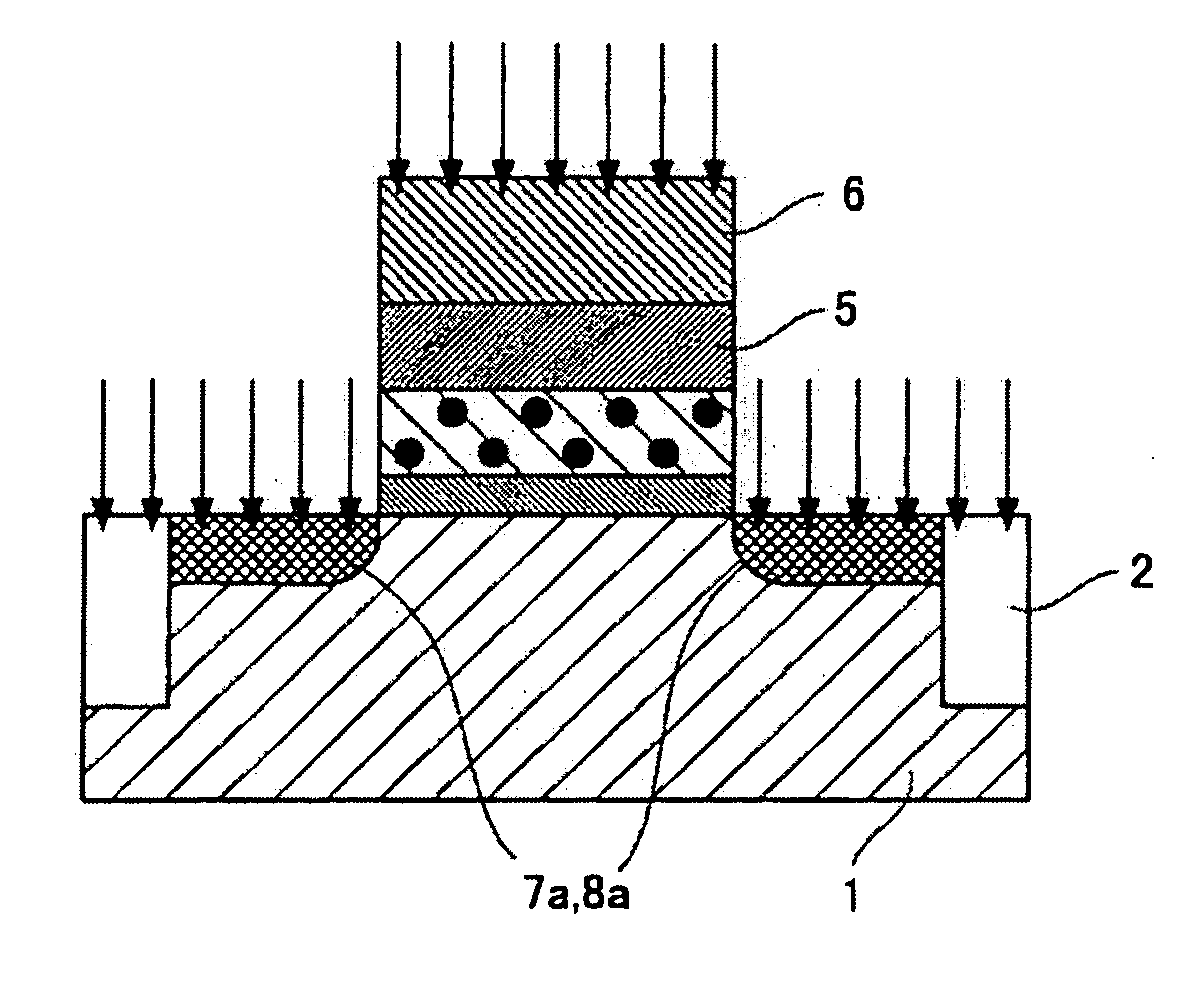
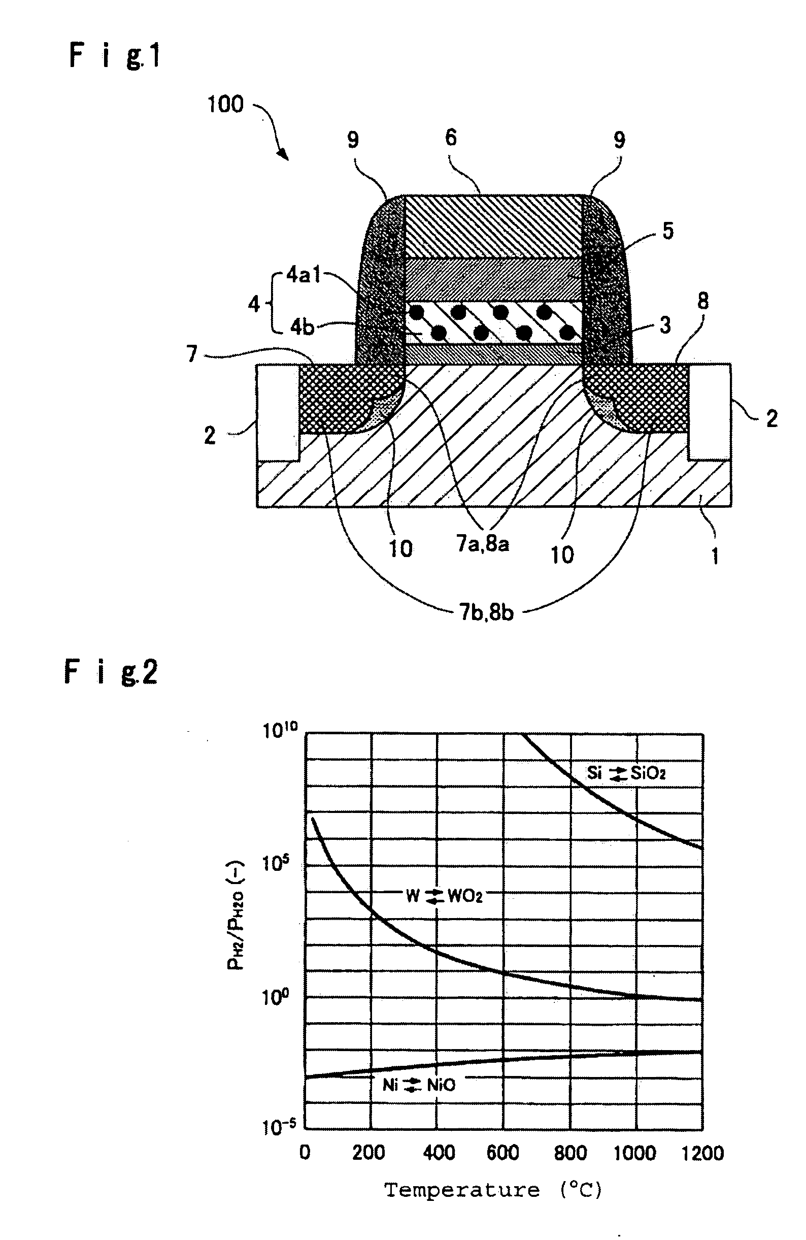
[0097]FIG. 1 is an explanation view schematically showing an example of cross sectional structure of a nonvolatile semiconductor memory element according to an embodiment of the present invention. In FIG. 1, a nonvolatile semiconductor memory element 100 is formed on a semiconductor substrate 1, and is isolated by element isolation 2. Here, the semiconductor substrate 1 in FIG. 1 is a semiconductor substrate of p-type, and the element isolation 2 is one formed by using a STI (Shallow Trench Isolation) technique.

[0098]The nonvolatile semiconductor memory element 100 has a structure that on the semiconductor substrate 1, a tunnel insulation film 3, a charge retention layer 4 for retaining an electric charge, a gate insulation film 5 and a control gate 6 laminated in this order. The charge retention layer 4 has a structure that ultrafine particles 4a1 functioning as a floating gate is dispersed in a matrix insulator 4b with high density.

[0099]Here, the control gate 6 forms a channel on...

example 1

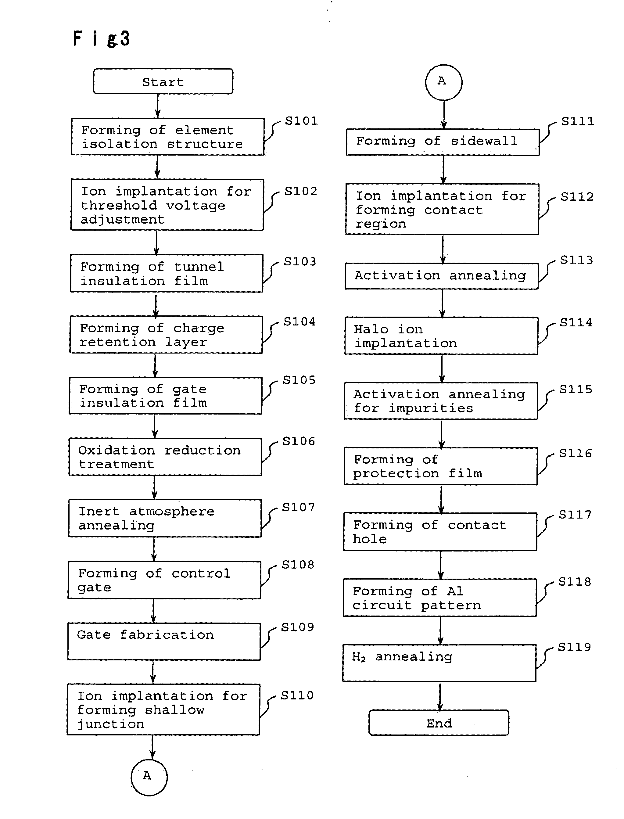
[0154]FIG. 3 is a process flow chart for explaining a process for producing nonvolatile semiconductor memory element according to Example 1. In this Example, process steps for producing peripheral circuit portions such as element selection transistors or signal amplification circuit, are omitted, and only process steps for producing memory elements are described.

[0155]First of all, element isolations 2 are formed on a surface of a semiconductor substrate 1 made of a single crystal Si doped with p-type impurities (S101; refer to FIG. 4). Then, ion implantation for adjusting threshold voltage is carried out (S102; refer to FIG. 5). Here, before this ion implantation, a film called as screen oxide film 21 schematically shown in FIG. 5 is formed by using Si thermal oxidation. As ions to be implanted, BF2+ ions are employed, and the semiconductor substrate is tilted by 7° to the incident direction of implanted ions so that the implanted ions do not cause channeling of the semiconductor s...

example 2

[0173]FIG. 17 is an explanation view schematically showing an example of cross sectional structure of a nonvolatile semiconductor memory element according to Example 2. First of all, in the same manner as explained in Example 1, on a surface of a semiconductor substrate 1 made of single crystal Si doped with p-type impurities, element isolations 2 are formed (S101; refer to FIG. 4), and ion implantation is carried out to adjust threshold voltage (S102; refer to FIG. 5).

[0174]Then, the above-mentioned screen oxide film 21 (refer to FIG. 5) is removed so that the surface of the semiconductor substrate 1 is exposed, and a tunnel insulation film 23 is formed on the surface of the semiconductor substrate 1 (S103; refer to FIG. 18). The forming of the tunnel insulation film 23 is carried out by thermally oxidizing and nitriding the surface of the semiconductor substrate 1 in a N2O atmosphere to form a SiO0.5N film. Here, the thickness of the tunnel insulation film 23 is made to be 3 nm.

[0...


PUM


Abstract

A nonvolatile semiconductor memory element enabling to improve insulation performance of an insulator around a floating gate and to decrease the ratio of oxidized metal ultrafine particles in the floating gate, are provided.
In a process for producing nonvolatile semiconductor memory element comprising a floating gate made of a hardly oxidizable material having a Gibbs' formation free energy for forming its oxide higher than that of Si in a range of from 0° C. to 1,200° C., and an insulator made of an oxide of an easily oxidizable material surrounding the floating gate and having such an energy equivalent or lower than that of Si, the floating gate made of hardly oxidizable material is formed by using a physical forming method, the oxide of the easily oxidizable material is formed by using a physical forming method or a chemical forming method, and after a gate insulation film is formed, a heat treatment is carried out in a mixed atmosphere of an oxidizing gas and a reducing gas in a temperature range of from 0° C. to 1,200° C. while the mixture ratio of the mixed gas and the temperature are controlled so that only the hardly oxidizable material is reduced and only the oxide of the easily oxidizable material is oxidized.

Description

TECHNICAL FIELD[0001]The present invention relates to a nonvolatile semiconductor memory element excellent in charge retention properties, which has a construction constituted by a plurality of materials containing elements having different Gibbs' formation free energies for forming oxides, that are different from one another by a difference in a level of the difference between those of Si and a transition metal such as Ni, W or Co; and to a process for producing such a device. The present invention particularly relates to a nonvolatile semiconductor memory element excellent in charge retention properties, which has the above construction constituted by a hardly oxidizable material and an oxide of easily oxidizable material, which is produced by decreasing defects in the oxide due to oxygen-shortage such as oxygen-shortage type defects or free valencies, by oxidation, and reducing the hardly oxidizable material. Hereinafter Gibbs' formation free energy for forming an oxide is also s...

Claims


Application Information

Patent Timeline
IPC IPC(8): H01L21/8234H01L21/336
CPCH01L21/28273H01L21/3105H01L21/316H01L29/7881H01L29/42332H01L29/66825H01L21/31645H01L29/40114H01L21/02181H01L21/02107
Inventor TAKATA, MASAAKIKOYANAGI, MITSUMASA
Owner ASAHI GLASS CO LTD
Why Eureka
Try Eureka