Supercharge Your Innovation With Domain-Expert AI Agents!

Low voltage diode with reduced parasitic resistance and method for fabricating

Active Publication Date: 2008-07-24
CREE INC
View PDF12 Cites 22 Cited by
  • Summary
  • Abstract
  • Description
  • Claims
  • Application Information

AI Technical Summary

Benefits of technology

[0019]This invention provides a semiconductor diode structure and method for fabrication a diode structure that substantially reduces parasitic resistance in the diode and eliminates the associated resistive voltage drops.
[0022]A third method of making a diode is similar to the second method, except that the substrate is a GaN substrate and that, after selective portions of the n+ and n− layers are removed to form a mesa diode structure, the GaN substrate is thinned to reduce parasitic substrate resistance and the ohmic contact is deposited on the thinned substrate.

Problems solved by technology

The width of the depletion zone, however, cannot grow without limit.
Beyond this point, a process called reverse breakdown occurs, which causes the device to be damaged, accompanied by a large increase in current.
One disadvantage of a junction diode is that, during forward conduction, the power loss in the diode can become excessive for large current flow.
Reducing the barrier potential, however, results in a tradeoff of increased reverse leakage current.
In addition, the reduced barrier can degrade high temperature operation and result in soft breakdown characteristics under reverse bias operation.
In addition, for Schottky diodes that are made of GaAs; one disadvantage of this material is that the Fermi level (or surface potential) is fixed or pinned at approximately 0.7 volts.
This additional voltage drop is unacceptable, since the target for total voltage drop at operating current is <200 mV.
Furthermore, for the most commonly used SiC substrate (GaN substrates are expensive and small in diameter), an additional barrier is encountered at the GaN epi-SiC substrate interface.
While there are techniques used to mitigate this barrier, they add extra complexity and may also contribute to increased resistance.

Method used


Image

  • Low voltage diode with reduced parasitic resistance and method for fabricating
  • Low voltage diode with reduced parasitic resistance and method for fabricating
  • Low voltage diode with reduced parasitic resistance and method for fabricating

Examples


second embodiment

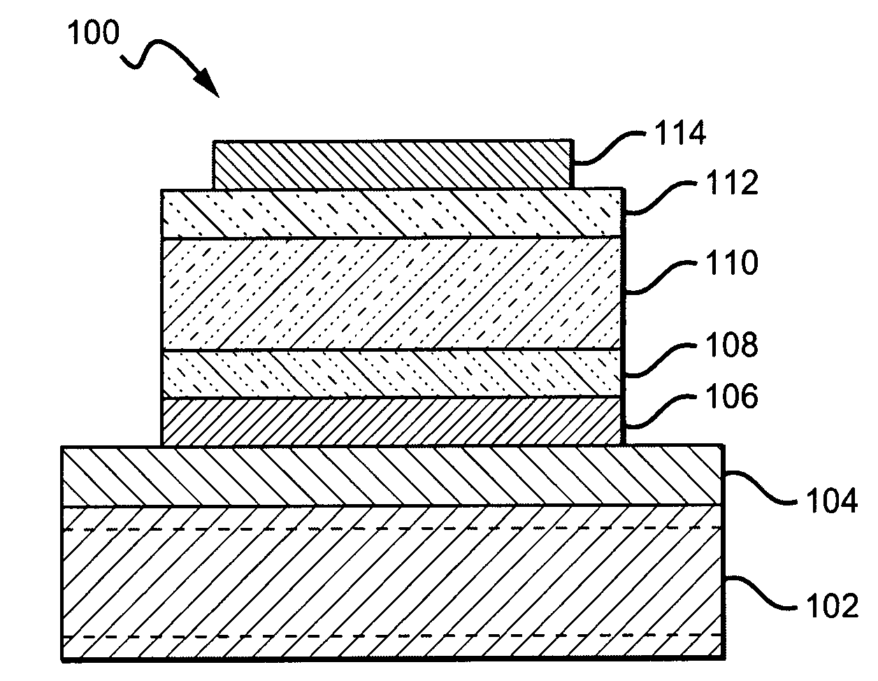
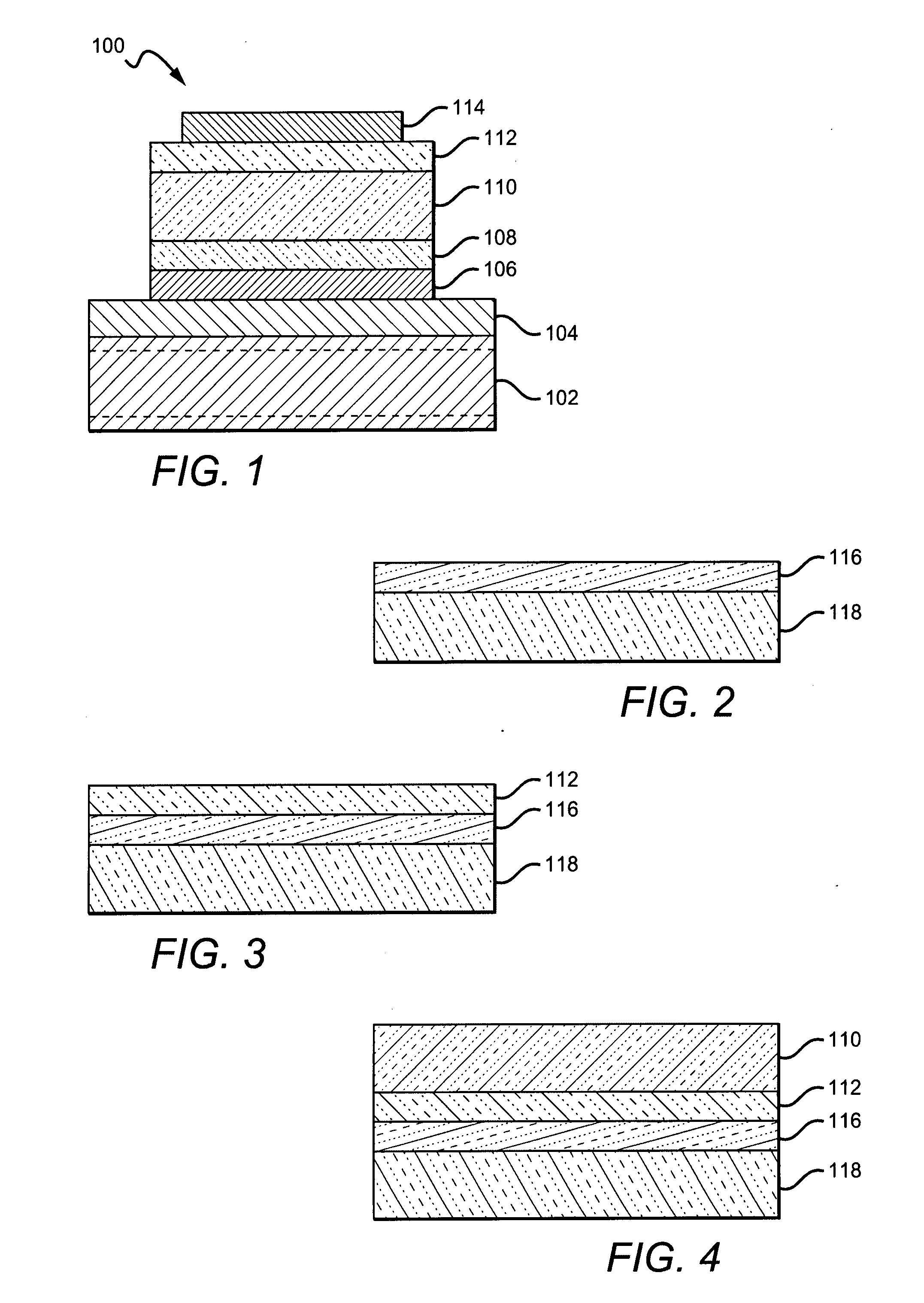
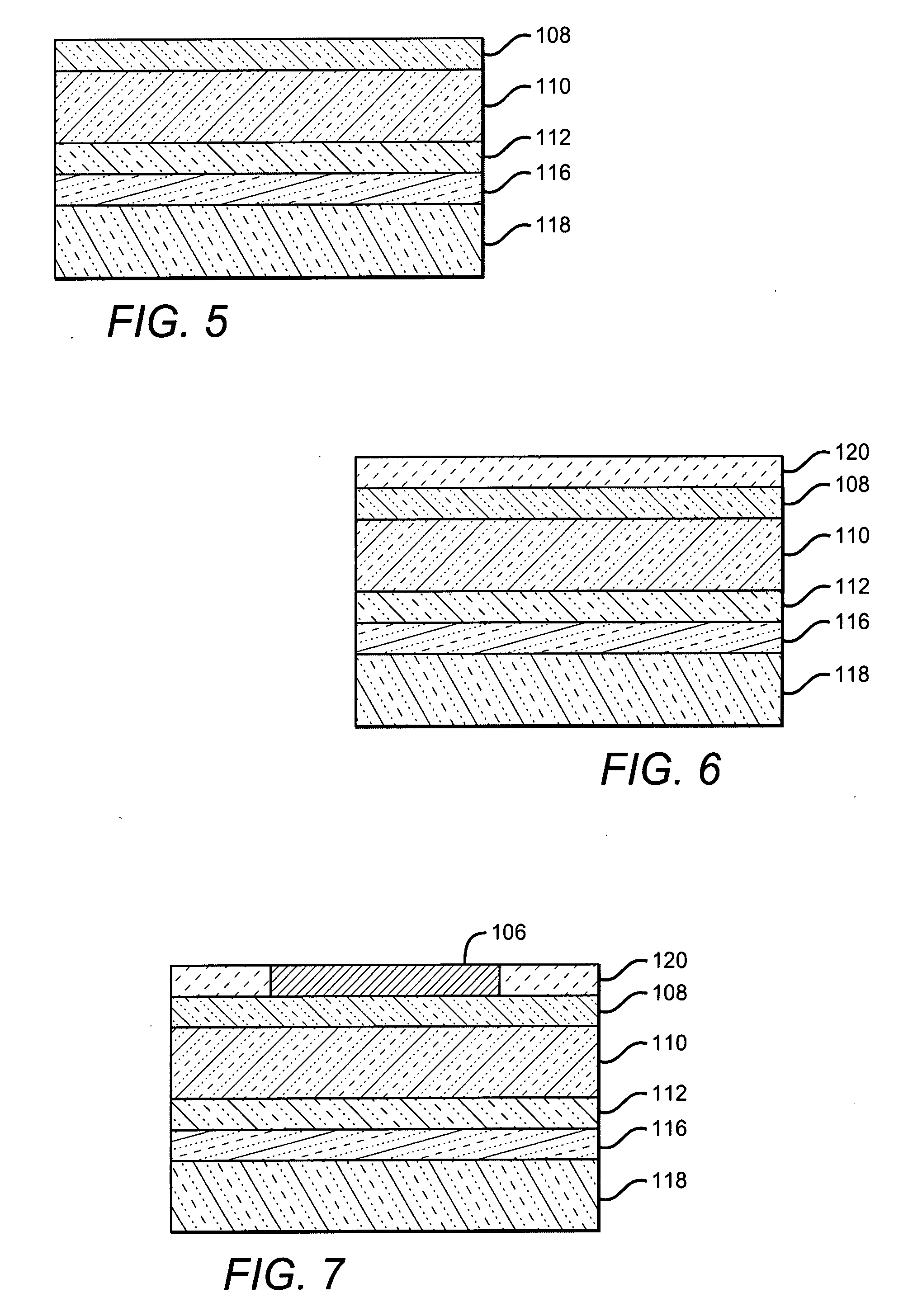
[0053]The diode of the invention can also be made in alternative embodiments. Instead of complete removal of the substrate, for example, a via can be etched in the substrate to remove the material under the active device and to retain the remainder of the substrate material for mechanical support. A diode 200, made according to this second embodiment, is depicted in FIG. 13, which is similar to FIG. 1. The diode 200 is fabricated in a manner similar to the process described in conjunction with FIGS. 2 through 7. A nucleation layer 216 is deposited on a SiC substrate 218, then an n+ semiconducting buffer layer 212 is deposited on the nucleation layer. An n− semiconducting layer 210 is deposited on the buffer layer 212 and a semiconducting barrier layer 208 is deposited on the n− layer 210. A Schottky metal layer 206 is deposited on the barrier layer 208.

[0054]Selected portions of the n+, n−, and buffer layers are then removed to form a mesa diode structure under the Schottky metal. F...

third embodiment

[0055]the diode can be implemented on a bulk GaN wafer, with the bulk GaN wafer being subsequently thinned to reduce parasitic substrate resistance. The bulk GaN wafer does not need to be completely removed since there is no heterostructure epi-substrate interface, as with the GaN diode fabricated on a SiC substrate. Other than the elimination of this interfacial voltage drop, reduction of substrate parasitic will be a function of the extent of thinning of the GaN substrate wafer.

[0056]The third embodiment is shown as the diode 300, as depicted in FIG. 14, which is also similar to FIG. 1. This embodiment, like the second embodiment, is fabricated using a process similar to that described in conjunction with FIGS. 2 through 7. A nucleation layer 316 is deposited on a GaN substrate 318, then an n+ semiconducting buffer layer 312 is deposited on the nucleation layer. An n− semiconducting layer 310 is deposited on the buffer layer 312 and a semiconducting barrier layer 308 is deposited ...


PUM


Abstract

A method of making a diode begins by depositing an AlxGa1−xN nucleation layer on a SiC substrate, then depositing an n+ GaN buffer layer, an n− GaN layer, an AlxGa1−xN barrier layer, and an SiO2 dielectric layer. A portion of the dielectric layer is removed and a Schottky metal deposited in the void. The dielectric layer is affixed to the support layer with a metal bonding layer using an Au-Sn utectic wafer bonding process, the substrate is removed using reactive ion etching to expose the n+ layer, selected portions of the n+, n−, and barrier layers are removed to form a mesa diode structure on the dielectric layer over the Schottky metal,; and an ohmic contact is deposited on the n+ layer.

Description

GOVERNMENT RIGHTS[0001]This invention was made with Government support under DARPA Contract No. 4400129974 (as subcontractor-Raytheon as prime). The Government has certain rights in this inventionBACKGROUND OF THE INVENTION[0002]This invention is concerned with diodes, and more particularly diodes exhibiting low on-state forward voltage and reduced parasitic resistance.[0003]A diode is an electronic component that restricts the direction of movement of charge carriers. The diode essentially allows an electric current to flow in one direction, but substantially blocks current flow in the opposite direction.[0004]Diode rectifiers are one of the most widely used devices in low voltage switching, power supplies, power converters and related applications. For efficient operation, it is desirable for such diodes to operate with low on-state voltage (a forward voltage drop Vf of 0.1-0.4V or lower), low reverse leakage current, a voltage blocking capability of 20-30V, and high switching spe...

Claims


Application Information

Patent Timeline
IPC IPC(8): H01L33/00H01L21/00
CPCH01L29/66143H01L29/66212H01L29/475H01L29/872H01L29/2003
Inventor PARIKH, PRIMITHEIKMAN, STEN
Owner CREE INC
Features
  • R&D
  • Intellectual Property
  • Life Sciences
  • Materials
  • Tech Scout
  • Unparalleled Data Quality
  • Higher Quality Content
  • 60% Fewer Hallucinations
Learn More