Nitride/zinc oxide based light-emitting diodes

a technology of nitride and zinc oxide, which is applied in the direction of semiconductor devices, basic electric elements, electrical apparatus, etc., can solve the problems of poor absorption and conversion efficiency of conventional phosphors used in fluorescent lighting, poor light-emitting performance, and high dislocation density of active layers

Inactive Publication Date: 2008-07-31
GEORGIA TECH RES CORP
View PDF0 Cites 17 Cited by
  • Summary
  • Abstract
  • Description
  • Claims
  • Application Information

AI Technical Summary

Benefits of technology

[0009]To overcome the problems noted above with respect to p-type ZnO, an embodiment of the invention comprises an alternative p-type GaN for a heterojunction device to take advantage of the fact that the a-lattice parameter of ZnO (a0=3.250, c0=5.207 Å) is close to that of GaN (a0=3.189, c0=5.185 Å), and that ZnO can be lattice-matched to In0.18Ga0.82N. Therefore, p-type GaN, In0.18Ga0.82N, and n-ZnO can be interfaced together in a heterojunction device without creating dislocations or other defects at the interfaces between the different materials which would have the undesirable effect of reducing the efficiency of the device.

Problems solved by technology

Conventional phosphors used in fluorescent lighting are not ideal for solid-state lighting because they have poor absorption and conversion efficiency.
However, these long wavelength LEDs based on nitride quantum well active layers experience higher dislocation density, increased point defects, and severe indium (In) phase separation.
Therefore, low internal quantum efficiency is expected for long wavelength LEDs based on nitride materials.
However, the reliability of p-type ZnO is still controversial [LOOK, D.C. et al., “P-type doping and devices based on ZnO,” Phys.
S55-S61, IOP Publishing Ltd., Bristol, United Kingdom] are still problems for implementing high-performance of ZnO based applications.

Method used


Image

  • Nitride/zinc oxide based light-emitting diodes
  • Nitride/zinc oxide based light-emitting diodes
  • Nitride/zinc oxide based light-emitting diodes

Examples


Embodiment Construction

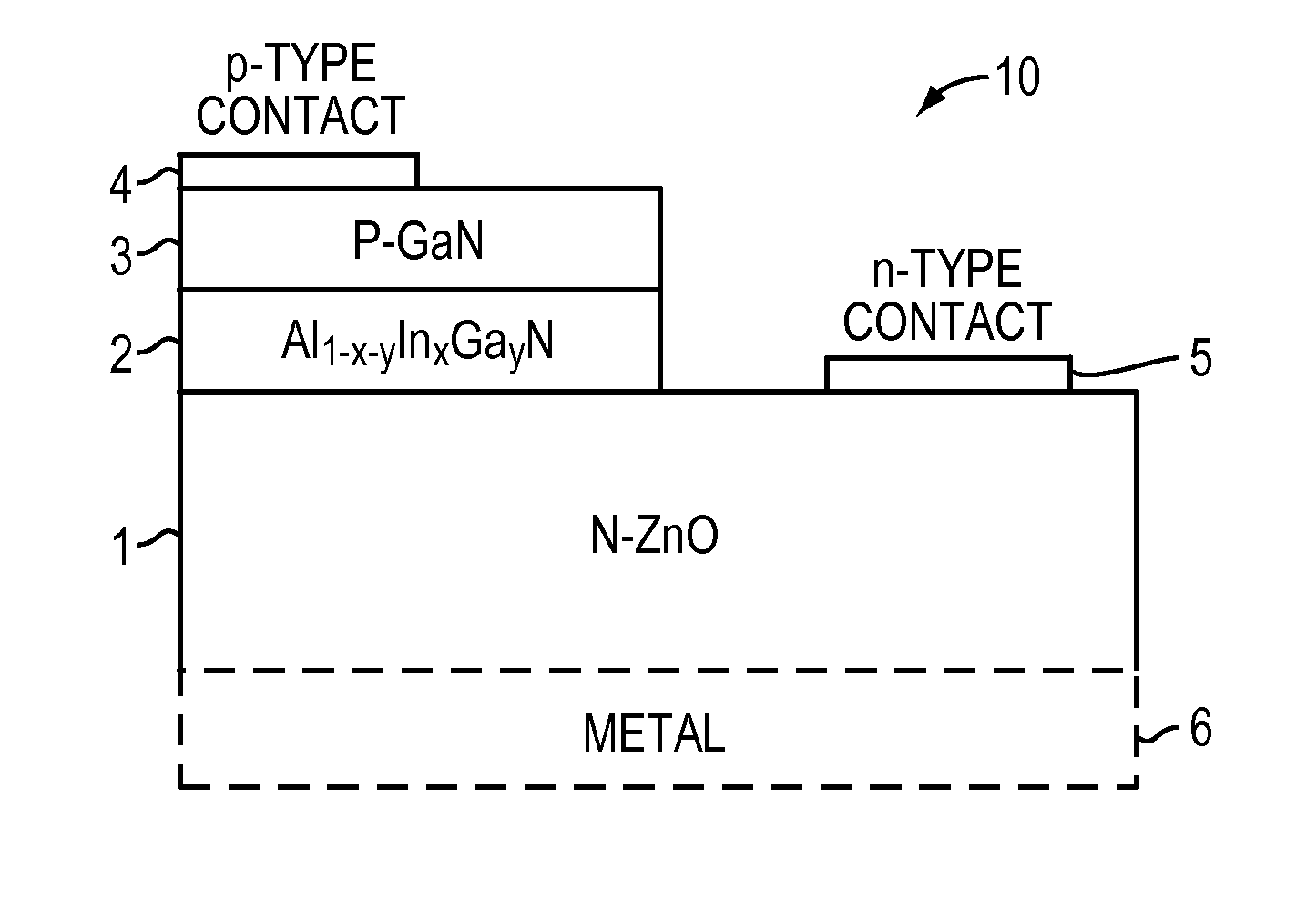
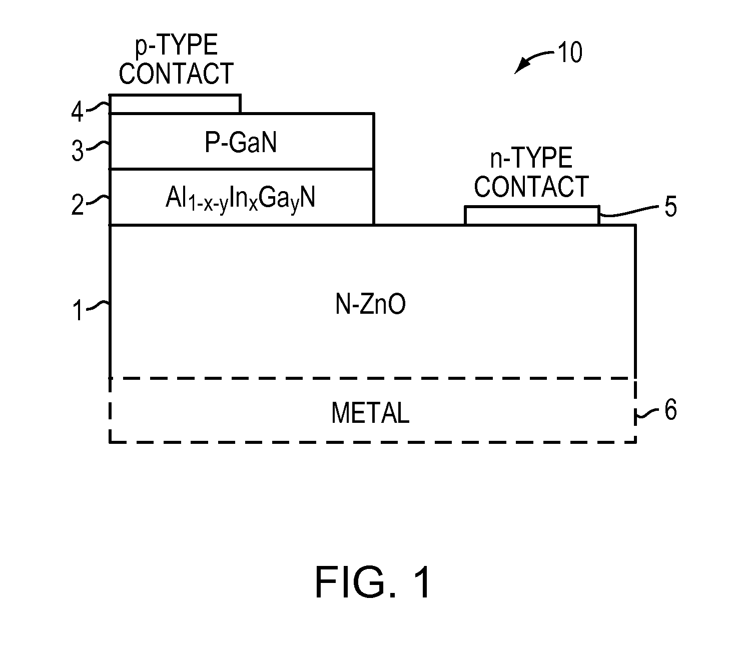
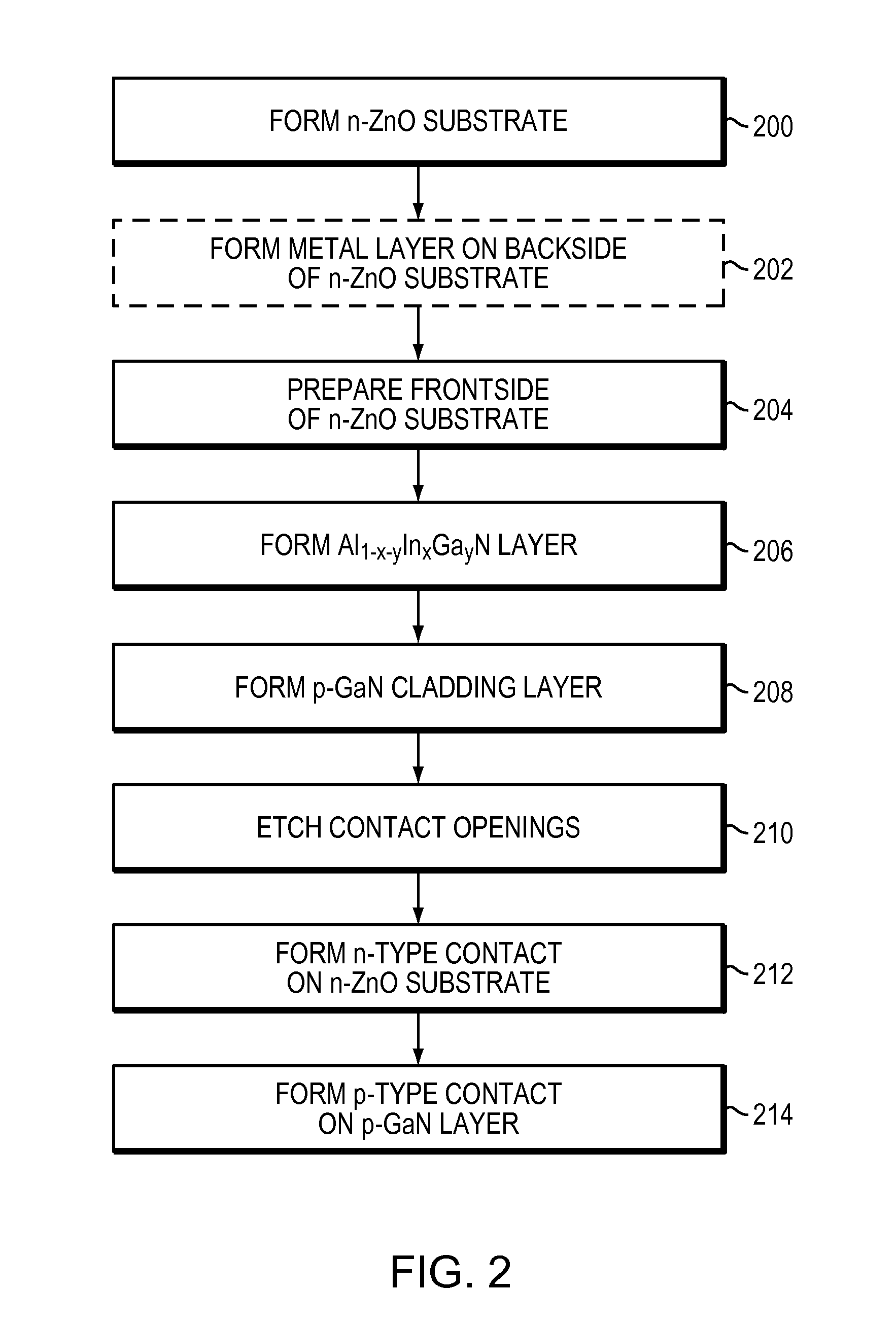
[0019]A detailed description of various embodiments of the device structures and methods of making such structures are provided below. The device 10 can be formed using a sputtering system, molecular beam epitaxy (MBE) system, metal organic chemical vapor deposition (MOCVD) system, hydride or halide vapor phase epitaxy (HVPE) system or other suitable system using known techniques. Suitable reactants, precursors, inert gases, etchants, resists, developers, mass flow controllers and other equipment necessary to make the device 10 as described herein are known in the art or can be readily employed based on the subject specification.

Structure of Light-Emitting Device with Homogeneous Active Layer

[0020]As shown in FIG. 1 the device 10 comprises an n-type zinc oxide (n-ZnO) layer or substrate 1, an active light-emitting layer 2 composed of Al1-x-yInxGayN; 0≦x3. The n-ZnO layer 1 is positioned in direct contact with the Al1-x-yInxGayN layer 2. Alternatively, the n-ZnO layer 1 may be positi...


PUM


Abstract

A light-emitting nitride / zinc oxide based compound semiconductor device of double heterostructure. The double-heterostructure includes a light-emitting layer formed of an Al1-x-yInxGayN; 0≦x<1, 0<y≦1, and x+y=0.1 to 1 compound semiconductor doped an impurity. Single or multi quantum well light-emitting active layers Al1-x-yInxGayN / GaN; 0≦x<1, 0<y≦1, and x+y=0.1 to 1 are positioned between p-type GaN and n-type ZnO substrates.

Description

CROSS-REFERENCE TO RELATED APPLICATIONS[0001]This patent application is a continuation-in-part claiming priority benefits under 35 U.S.C. §120 to U.S. Nonprovisional application Ser. No. 11 / 939,553 filed Nov. 14, 2007 and U.S. Nonprovisional application Ser. No. 11 / 938,764 filed Nov. 12, 2007 which claims priority benefits under 35 U.S.C. §119(e) to U.S. Provisional Application No. 60 / 858,574 filed Nov. 13, 2006, all of which name Gon Namkoong and William Alan Doolittle as inventors, and which are all incorporated by reference herein.BACKGROUND OF THE INVENTION[0002]1. Field of the Invention[0003]The present invention relates to a phosphor-free light-emitting heterojunction nitride / zinc oxide based compound semiconductor device. More particularly, it relates to a light-emitting compound semiconductor device implemented by energy band gap engineering of nitride and zinc oxide semiconductor materials to emit longer wavelengths ranging from green to orange to red (a wavelength range of...

Claims


Application Information

Patent Timeline
Patent Type & Authority Applications(United States)
IPC IPC(8): H01L33/00H01L33/02H01L33/26H01L33/32
CPCH01L33/007H01L33/32H01L33/26H01L33/02
Inventor NAMKOONG, GONDOOLITTLE, WILLIAM ALAN
Owner GEORGIA TECH RES CORP
Why Eureka
Try Eureka