Control method for optical phase modulation

a control method and optical phase technology, applied in the field of optical communication, can solve the problems of inability to apply conventional technology to optical modulators, inability to apply intensity modulators but cannot apply to optical qpsk modulators, and low two-photon absorption probability, so as to stabilize the operation stabilize modulation characteristics, and stabilize the effect of optical qpsk modulators

Inactive Publication Date: 2008-07-31
HITACHI COMM TECH
View PDF2 Cites 38 Cited by
  • Summary
  • Abstract
  • Description
  • Claims
  • Application Information

AI Technical Summary

Benefits of technology

[0028]According to an aspect of this invention, it is possible to: stabilize a phase shift amount (to π / 2 for example) by applying feedback to a drive voltage that determines the phase shift amount of a phase shifter; and thus stabilize the operations of an optical QPSK modulator. Further, it is possible to: stabilize a modulation characteristic by applying feedback to drive signals (a DC bias for example) of a phase modulator even when the modulation characteristic of the phase modulator drifts; and thus stabilize the operations of an optical QPSK modulator. As a result, a stable communication system can be established.

Problems solved by technology

However, in the case of an optical modulator made of a material other than a compound semiconductor, e.g. LN as a ferroelectric material, two-photon absorption probability is very low and the conventional technology cannot be applied to the optical modulator.
However, the means is effective for an intensity modulator but cannot be applied to an optical QPSK modulator.

Method used


Image

  • Control method for optical phase modulation
  • Control method for optical phase modulation
  • Control method for optical phase modulation

Examples


embodiment 1

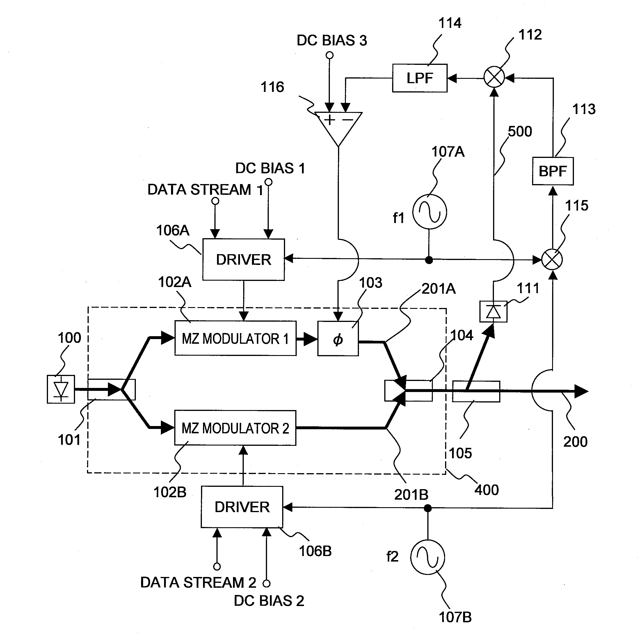
[0047]Firstly, an optical QPSK modulator of a first embodiment according to this invention is explained with FIG. 1.

[0048]Continuous light outputted from a laser 100 is branched into two streams with a 1:2 optical coupler (with one input and two outputs) 101. The branched light is inputted into MZ modulators 102A and 102B respectively. The MZ modulator 102A modulates the phase of the light to “0” and “π” in accordance with the digital signals “0” and “1” of an information data stream 1.

[0049]A driver 106A converts the information data stream 1 into a drive voltage pulse stream so that the MZ modulator 102A may operate as a phase modulator. The driver 106A adds a DC bias 1 to the drive voltage pulse stream. FIG. 5 shows concrete setting of a voltage amplitude and a DC bias. Further, the driver 106A applies amplitude modulation to the drive pulse stream with the signals of frequency f1 outputted from an oscillator 107A. The frequency f1 is set a frequency sufficiently lower than the b...

embodiment 2

[0067]A second embodiment will be described hereinafter. The second embodiment has the same circuit configuration of the optical QPSK modulator as that of the first embodiment but the method for applying amplitude modulation to drive voltage signals of the MZ modulators is different. More specifically, the relationship between drive voltage signals and a modulation characteristic of an MZ modulator in the second embodiment is shown in FIG. 9.

[0068]In the second embodiment, the phase of the amplitude modulation at the drive voltage signal level where the phase of light is “0” (V1−V2=0 in FIG. 9) is identical to the phase of the amplitude modulation at the drive voltage signal level where the phase of light is “π” (V1−V2=2Vπ in FIG. 9). Note that, in the aforementioned first embodiment, the phases at the drive voltage signal levels in the cases of “0” and “π” are opposite as shown in FIG. 8.

[0069]In the case of the second embodiment, the intensity of the difference frequency component...

embodiment 3

[0071]A third embodiment will be described hereinafter. The third embodiment is hereunder explained with FIG. 10. In the third embodiment, unlike the aforementioned first embodiment, the drift phenomenon of the modulation characteristics of the two MZ modulators is compensated by using low frequency signals (frequencies f1 and f2) outputted from the two oscillators 107A and 107B.

[0072]More specifically, in the drive voltage signals applied to the two MZ modulators 102A and 102B, similarly to the aforementioned second embodiment, the phases of the amplitude modulation of the low frequency signals (frequency f0) applied to the drive signal level of phase “0” and the drive signal level of phase “π” shown in FIG. 9 are identical. In the case of the third embodiment, as shown in FIG. 11, when the modulation characteristics of the MZ modulators 102A and 102B drift, amplitude modulation of the frequency f0 is applied to the light outputted from the MZ modulators 102A and 102B. When the bia...


PUM


Abstract

A QPSK modulator comprising: two phase modulators implemented in parallel for outputting the light phase-modulated with an information signal; a phase shifter for shifting the phase of the light phase-modulated with the first phase modulator of the two phase modulators and for outputting the phase-shifted light; and a combiner for combining output light of the phase shifter and output light of the second phase modulator, in which a drive signal generated by multiplexing a signal of a first and second frequencies and the information signal is inputted into the first and second phase modulators, and in which the QPSK modulator feeds back a detected amount to a voltage applied to the phase shifter so that the phase shift amount may be π / 2, the detected amount of signals having the frequency of the difference between or the sum of the first and second frequency which are extracted from the modulated light.

Description

CLAIM OF PRIORITY[0001]The present application claims priority from Japanese patent application JP 2007-016333 filed on Jan. 26, 2007, the content of which is hereby incorporated by reference into this application.BACKGROUND OF THE INVENTION[0002]This invention relates to a method for optical communication, in particular to a method for modulating light used as carrier waves.[0003]A binary modulation technology using light intensity is applied to a current optical communication system. More specifically, “0” and “1” as digital information are converted to on and off of light intensity on the side of a sender and the converted information is transmitted to an optical fiber. The light having propagated in the optical fiber is photoelectrically converted and the original information is demodulated on the side of a receiver.[0004]In recent years, in proportion to the explosive popularization of the Internet, the channel capacity required for an optical communication system is extremely ...

Claims


Application Information

Patent Timeline
Patent Type & Authority Applications(United States)
IPC IPC(8): H04B10/04H04B10/40H04B10/07H04B10/50H04B10/516H04B10/524H04B10/54H04B10/556H04B10/60H04B10/61H04L27/18
CPCH04B10/5561H04B10/5053
Inventor SASAKI, SHINYA
Owner HITACHI COMM TECH
Why Eureka
Try Eureka