Plasma process uniformity across a wafer by apportioning ground return path impedances among plural vhf sources
What is AI technical title?
AI technical title is built by PatSnap AI team. It summarizes the technical point description of the patent document.
a vhf source and ground return path technology, applied in the direction of coatings, chemical vapor deposition coatings, electric discharge tubes, etc., can solve the problems of non-uniform process at the wafer surface, affecting the uniformity of the rf field, and the radial transmission line effect and loading of the ceiling electrod
Inactive Publication Date: 2008-07-31
APPLIED MATERIALS INC
View PDF13 Cites 14 Cited by
Summary
Abstract
Description
Claims
Application Information
AI Technical Summary
This helps you quickly interpret patents by identifying the three key elements:
Problems solved by technology
Method used
Benefits of technology
Benefits of technology
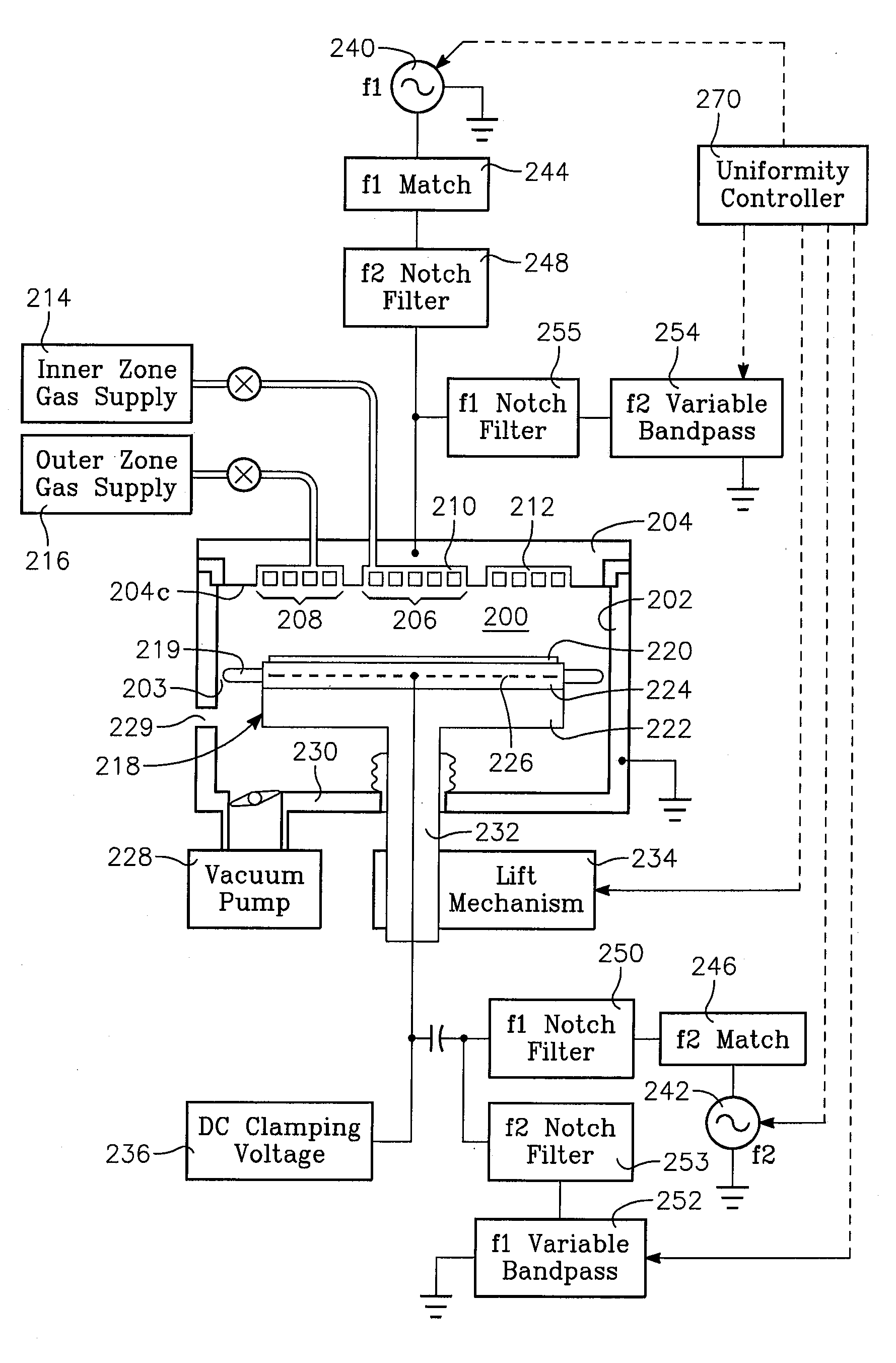
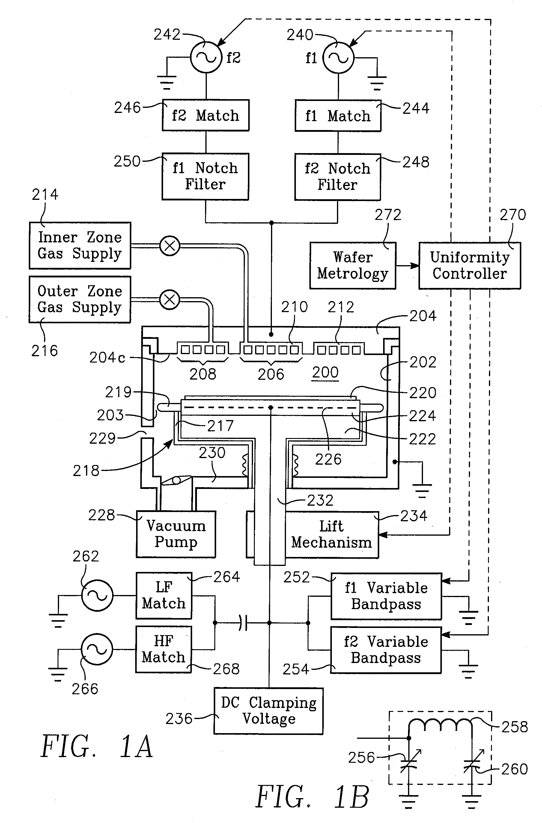
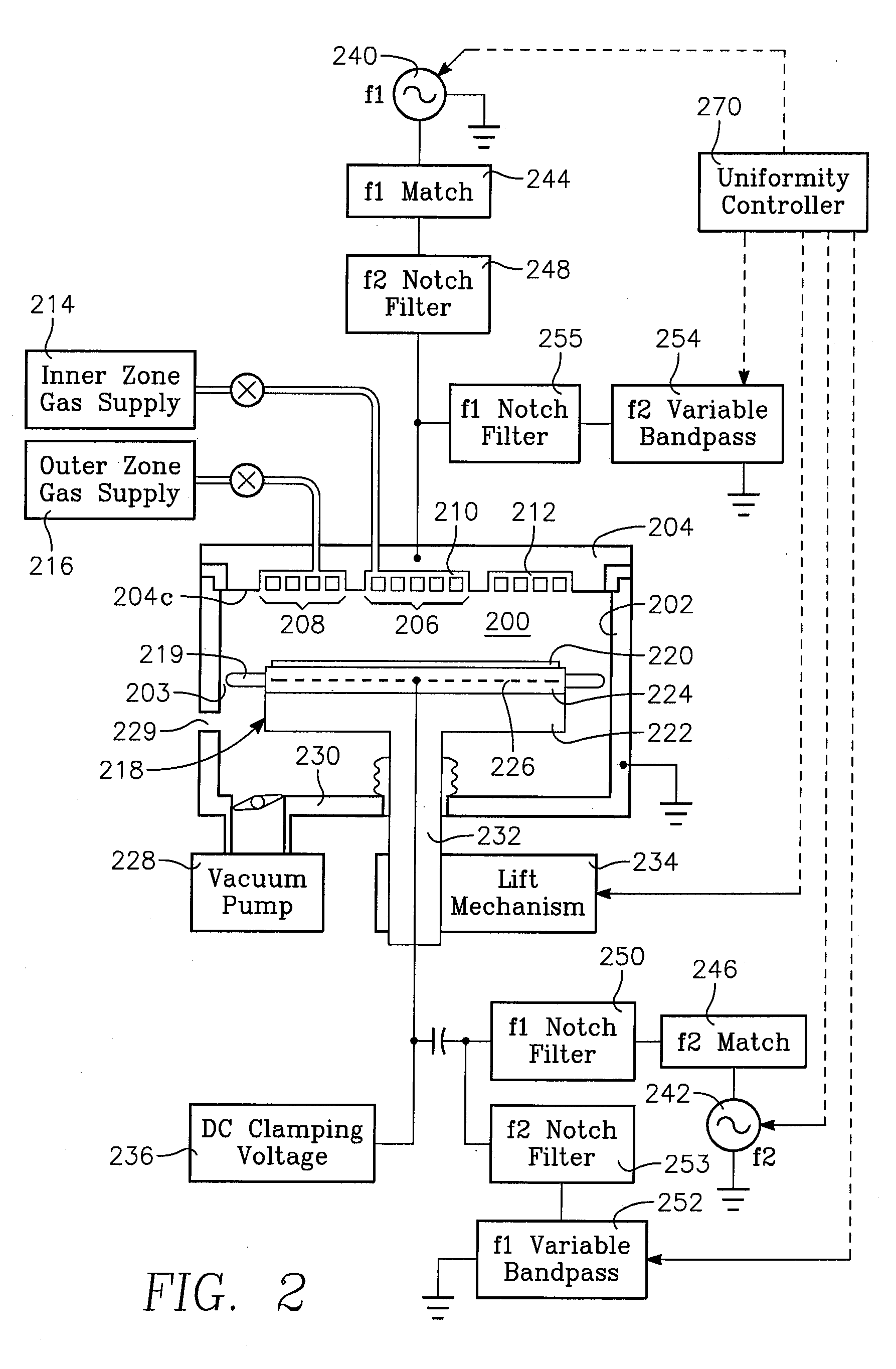
[0005]A method is provided for processing a workpiece in a plasma reactor chamber having electrodes including at least a ceiling electrode and a workpiece support electrode. The method includes coupling respective RF power sources of respective VHF frequencies f1 and f2 to either respective ones of the electrodes or to a common one of the electrodes, where f1 is sufficiently high to produce a center-high non-uniform plasma ion distribution and f2 is sufficiently low to produce a center-low non-uniform plasma ion distribution. The method further includes providing respective center ground return paths for RF current passing directly between the ceiling electrode and the workpiece support electrode for the frequencies f1 and f2, and providing an edge ground return path for each of the frequencies f1 and f2. The method also includes adjusting the impedance of at least one of the ground return paths so as to control the uniformity of the plasma ion density distribution.
Problems solved by technology
One problem inherent in such a plasma source is that the ceiling electrode exhibits radial transmission line effects and loading due to the effective dielectric constant of the plasma.
Therefore, the RF field varies significantly across the surface of the ceiling electrode, giving rise to process non-uniformities at the wafer surface.
For a plasma with an effective dielectric constant greater than 1 , the effective wavelength is reduced to less than the ceiling electrode diameter, worsening the non-uniformity of the RF field, making processing non-uniformities across the wafer surface worse.
For an etch process, this may produce a non-uniform edge low etch rate distribution across the wafer surface.
One problem with this approach is that a center-high non-uniformity of the source may be beyond the corrective capability of magnetic steering.
Another problem with this approach can be electrical charging damage of the workpiece if the magnetic flux density is too high.
The net effect is to reduce the effect of the dielectric constant of the plasma, thereby reducing the non-uniformity of the RF field.
However, a high plasma bias voltage is not desirable in some other types of plasma processes.
The worst non-uniformities appear in processes employing the lowest plasma bias voltage.
Such approaches are complicated by the fact that other process conditions dictated by the process recipe have as great an effect upon plasma distribution as either magnetic steering or bias (sheath) voltage.
Method used
Image
Click on the blue label to locate the original text in one second.
Reading with bidirectional positioning of images and text.
Examples
Embodiment Construction
[0026]FIG. 1A is a simplified schematic diagram of a plasma reactor capable of controlling radial distribution of plasma ion density by apportioning capacitively coupled plasma source power among different source power frequencies. The reactor has a vacuum chamber 200 enclosed by a cylindrical side wall 202 and a disk-shaped ceiling 204. The ceiling 204 is both a conductive ceiling electrode as well as a gas distribution showerhead or plate, and will be referred to herein as the ceiling electrode 204. The ceiling electrode may optionally be covered with a conducting, semiconducting or insulating material. The ceiling electrode 204 includes inner and outer zones 206, 208 of gas injection orifices on its bottom surface 204c coupled to respective inner and outer internal gas manifolds 210, 212. Inner and outer zone process gas supplies 214, 216 furnish process gases to the inner and outer manifolds 210, 212. A wafer support pedestal 218 can support a workpiece such as a semiconductor w...
PUM
Property
Measurement
Unit
Density
aaaaa
aaaaa
Frequency
aaaaa
aaaaa
Density distribution function
aaaaa
aaaaa
Abstract
In a plasma reactor chamber a ceiling electrode and a workpiece support electrode, respective RF power sources of respective VHF frequencies f1 and f2 are coupled to either respective ones of the electrodes or to a common one of the electrodes, where f1 is sufficiently high to produce a center-high non-uniform plasmaion distribution and f2 is sufficiently low to produce a center-low non-uniform plasmaion distribution. Respective center ground return paths are provided for RF current passing directly between the ceiling electrode and the workpiece support electrode for the frequencies f1 and f2, and an edge ground return path is provided for each of the frequencies f1 and f2. The impedance of at least one of the ground return paths is adjusted so as to control the uniformity of the plasma iondensity distribution.
Application Information
Patent Timeline
Application Date:The date an application was filed.
Publication Date:The date a patent or application was officially published.
First Publication Date:The earliest publication date of a patent with the same application number.
Issue Date:Publication date of the patent grant document.
PCT Entry Date:The Entry date of PCT National Phase.
Estimated Expiry Date:The statutory expiry date of a patent right according to the Patent Law, and it is the longest term of protection that the patent right can achieve without the termination of the patent right due to other reasons(Term extension factor has been taken into account ).
Invalid Date:Actual expiry date is based on effective date or publication date of legal transaction data of invalid patent.
InventorCOLLINS, KENNETH S.HANAWA, HIROJIRAMASWAMY, KARTIKBUCHBERGER, DOUGLAS A.RAUF, SHAHIDBERA, KALLOLWONG, LAWRENCEMERRY, WALTER R.MILLER, MATTHEW L.SHANNON, STEVEN C.NGUYEN, ANDREWCRUSE, JAMES P.CARDUCCI, JAMESDETRICK, TROY S.DESHMUKH, SUBHASHSUN, JENNIFER Y.

