Undercut-free blm process for pb-free and pb-reduced c4

a blm and c4 technology, applied in the field of semiconductor chip fabrication, can solve the problems of limiting the extendibility of current electroetch blm technology, cu and tiw base layers are associated with undercutting of blm, etc., and achieves the effects of reducing pitch, reducing undercutting amount, and increasing mechanical stability of solder bump connection

Inactive Publication Date: 2008-08-14
ULTRATECH INT INC
View PDF12 Cites 87 Cited by
  • Summary
  • Abstract
  • Description
  • Claims
  • Application Information

AI Technical Summary

Benefits of technology

[0037]wherein said barrier material liner adjacent said solder bump connection exhibit decreased amo...

Problems solved by technology

The drive to Lead-reduced and lead-free C4 processing together with reduced-pitch requirements limit the extendibility of current electroetch BLM technology, which routinely produces a final structure in which the baselayer BLM films (Ti, Cu) are dimensionally inset or “undercut” with respect to the outer dimension of the C4 solder ball.
It is the case though, that problems associated with undercut of the BLM during wet electroetching of the Cu and TiW base layers exist.
For example, the final structure such as shown in FIG. 1D, is at risk for reliability failure due to the minimal effective contact attach area of the remaining TiW base layer to the final passivation (polyimide) film 12, and/or with respect to the voids created by undercut 50 at each edge of the str...

Method used


Image

  • Undercut-free blm process for pb-free and pb-reduced c4
  • Undercut-free blm process for pb-free and pb-reduced c4
  • Undercut-free blm process for pb-free and pb-reduced c4

Examples


Embodiment Construction

[0046]The process flow for forming a novel solder bump metallurgy according to the invention is now described with reference to FIGS. 2A-2C.

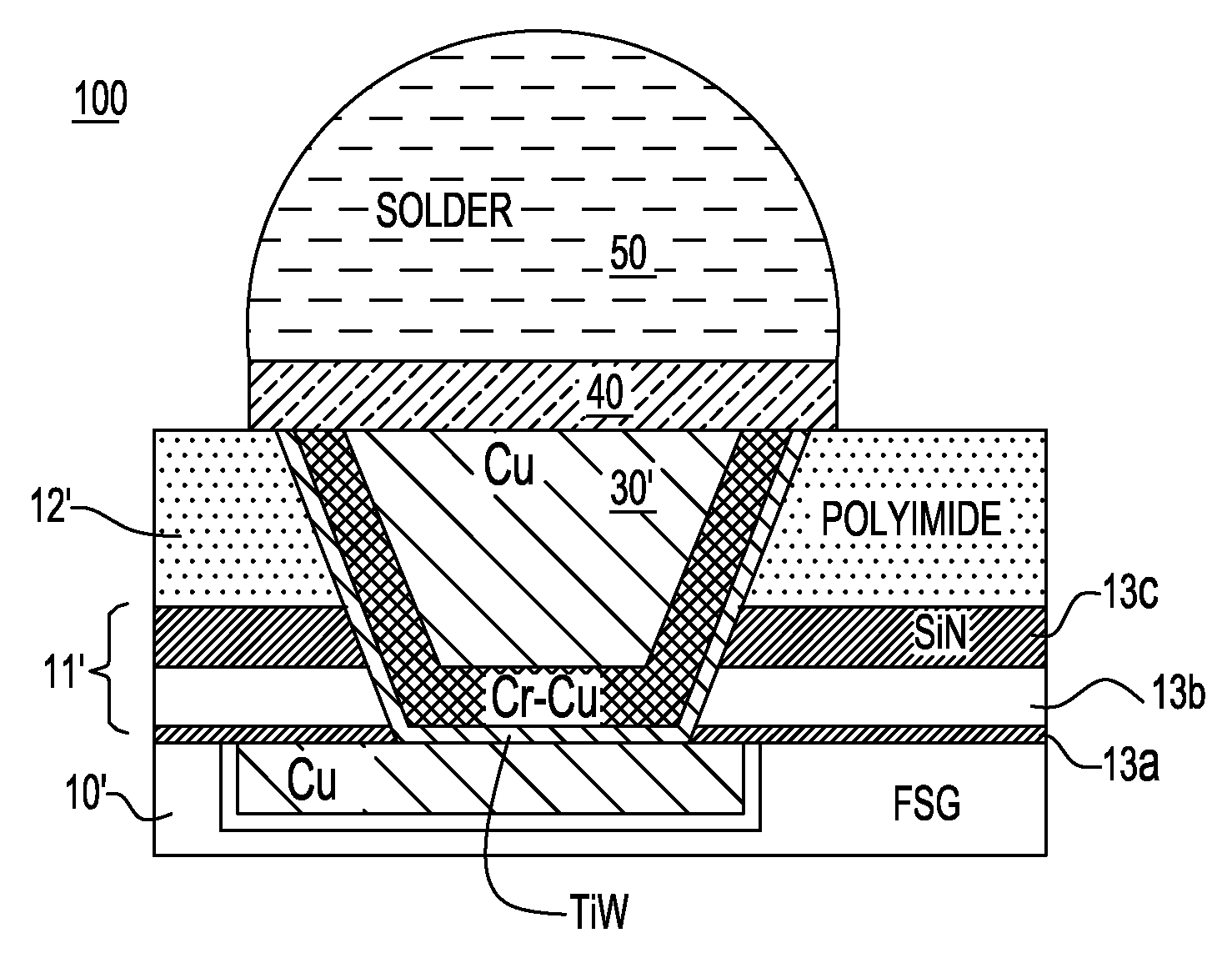
[0047]The process flow allows for the reliable fabrication of a BLM for Pb-Free and Pb-Reduced C4, without undercut. The process can be used with the TiW—Cu—Ni BLM and will solve the undercut problems. Alternatively, the disclosed process can also be used for a standard Pb-reduced BLM containing CrCu—e.g. TiW / CrCu / Cu / Ni. The process depends upon the replacement of electroetch of the Cu (and CrCu) and TiW layer with first a damascene CMP to create a localized Cu “plug” (or CrCu / Cu) only in the final via, and then a RIE process for TiW. The RIE process for TiW is successful because of the now complete removal of Cu (or CrCu) residues (normally present after wet or electroetching) in the field areas by CMP. The TiW—Cu layers are deposited by PVD, and the plug is formed by damascene CMP of Cu, stopping on the TiW. There are two embodiments from this...


PUM


Abstract

A system and method for eliminating undercut when forming a C4 solder bump for BLM (Ball Limiting Metallurgy) and improving the C4 pitch. In the process, a barrier layer metal stack is deposited above a metal pad layer. A top layer of the barrier layer metals (e.g., Cu) is patterned by CMP with a bottom conductive layer of the barrier metal stack removed by etching. The diffusion barrier and C4 solder bump may be formed by electroless plating, in one embodiment, using a maskless technique, or by an electroplating techniques using a patterned mask. This allows the pitch of the C4 solder bumps to be reduced.

Description

BACKGROUND OF THE INVENTION[0001]1. Field of the Invention[0002]The present invention relates generally to the fabrication of semiconductor chips, and more particularly to a structure and novel methodology for fabricating a reliable, dimensionally accurate, high-integrity Ball Limiting Metallurgy (BLM) without undercut in Back-End-Of-Line (BEOL) semiconductor chip processing.[0003]2. Description of the Prior Art[0004]Controlled Collapse Chip Connection (C4) processes are well known in forming solder bumps in back-end-of line semiconductor fabrication, e.g., when chips are connected to their packaging. Typically, the formation of a C4 solder bump includes the conventional formation of a metallurgical system that includes the underlying final metal layer (pad), an under “bump” or Ball Limiting Metallurgy (BLM) and the solder ball. The BLM ideally should provide good adhesion to a wafer passivation and to the IC final metal pad, and, function as an effective solder diffusion barrier.[0...

Claims


Application Information

Patent Timeline
IPC IPC(8): H01L21/44
CPCH01L23/3192H01L24/03H01L24/05H01L24/11H01L24/13H01L2224/03462H01L2224/03912H01L2224/0401H01L2224/05006H01L2224/0501H01L2224/05083H01L2224/05546H01L2224/05624H01L2224/114H01L2224/11462H01L2224/1147H01L2224/11472H01L2224/11474H01L2224/116H01L2224/11849H01L2224/13006H01L2224/13023H01L2224/1308H01L2224/13083H01L2224/131H01L2224/13147H01L2224/13155H01L2224/16H01L2924/01005H01L2924/01013H01L2924/01014H01L2924/01015H01L2924/01022H01L2924/01027H01L2924/01028H01L2924/01029H01L2924/01047H01L2924/0105H01L2924/01073H01L2924/01074H01L2924/01075H01L2924/01078H01L2924/01079H01L2924/01082H01L2924/014H01L2924/04953H01L2924/00013H01L2924/01006H01L2924/01019H01L2924/01023H01L2924/01024H01L2924/01033H01L2224/11902H01L2924/00014H01L2224/13099H01L2224/0361H01L2224/023H01L2924/0001H01L23/48
Inventor DAUBENSPECK, TIMOTHY H.GAMBINO, JEFFREY P.MUZZY, CHRISTOPHER D.SAUTER, WOLFGANG
Owner ULTRATECH INT INC
Why Eureka
Try Eureka