Casting method for polycrystalline silicon

a casting method and polycrystalline silicon technology, applied in the direction of polycrystalline material growth, crystal growth process, chemistry apparatus and processes, etc., can solve the problems of increasing the production cost of solar cells, increasing the production cost of single crystal silicon, so as to suppress the growth of the chill layer, reduce the current value, and delay the initiation of solidification

Inactive Publication Date: 2008-09-04
SUMCO CORP
View PDF7 Cites 16 Cited by
  • Summary
  • Abstract
  • Description
  • Claims
  • Application Information

AI Technical Summary

Benefits of technology

[0022]In the inner part of the ingot, semiconductor properties are excellent as a result of the existence of the columnar crystals 18a, 18b which have grown a large crystal diameter, whereas in chill layer 17, semiconductor properties cannot be excellent as a result of the small crystal diameter and plenty of crystalline defects. For this reason, in order to improve the conversion efficiency of cast polycrystalline silicon used as solar cells, the need arises to suppress the growth of chill layer 17. As this chill layer 17 occurs on the ingot surface with its high solidification speed, the growth of chill layer 17 can be suppressed by mitigating the rapid cooling of the ingot surface at the time of solidifying the molten silicon and producing the ingot, that is, by maintaining the surface temperature at high temperatures in order to delay the initiation of solidification caused by cooling from the ingot surface.
[0038]In this way, according to the casting method for polycrystalline silicon of the present invention, it is possible to suppress the deterioration of semiconductor properties of the inner part and surface of the ingot, with the result that it becomes possible to increase the conversion efficiency as solar cells.

Problems solved by technology

However, single crystal silicon grown with the Czochralski method has the disadvantage of incurring higher production costs when compared with polycrystalline silicon discussed hereafter.
Consequently, the use of single crystal silicon as substrates for solar cells causes the problem of increasing production costs for solar cells.
By applying a unidirectional solidification method in this casting method, it becomes possible to obtain polycrystalline silicon with large crystal grains, but as the casting method is an ingot casting method whereby the molten silicon is solidified with the mold, various problems arise.
As stated above, the fact that high-purity materials such as quartz crucibles and graphite molds are used in the casting method in addition to the need for these to be replaced periodically, leads to a rise in production costs.
Moreover, the casting method is an ingot casting method, and difficulties with continuous casting result in a decrease in the production efficiency.

Method used


Image

  • Casting method for polycrystalline silicon
  • Casting method for polycrystalline silicon
  • Casting method for polycrystalline silicon

Examples


examples

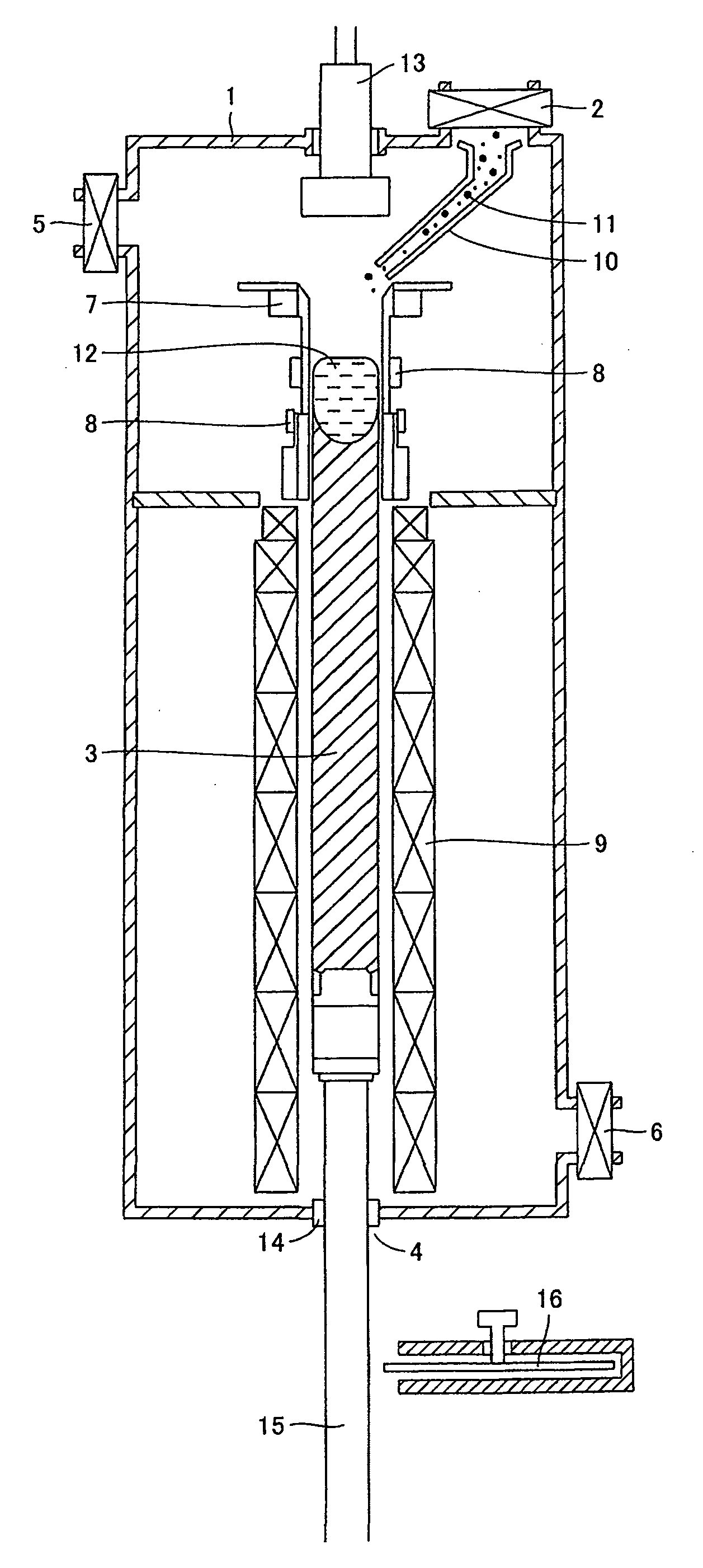
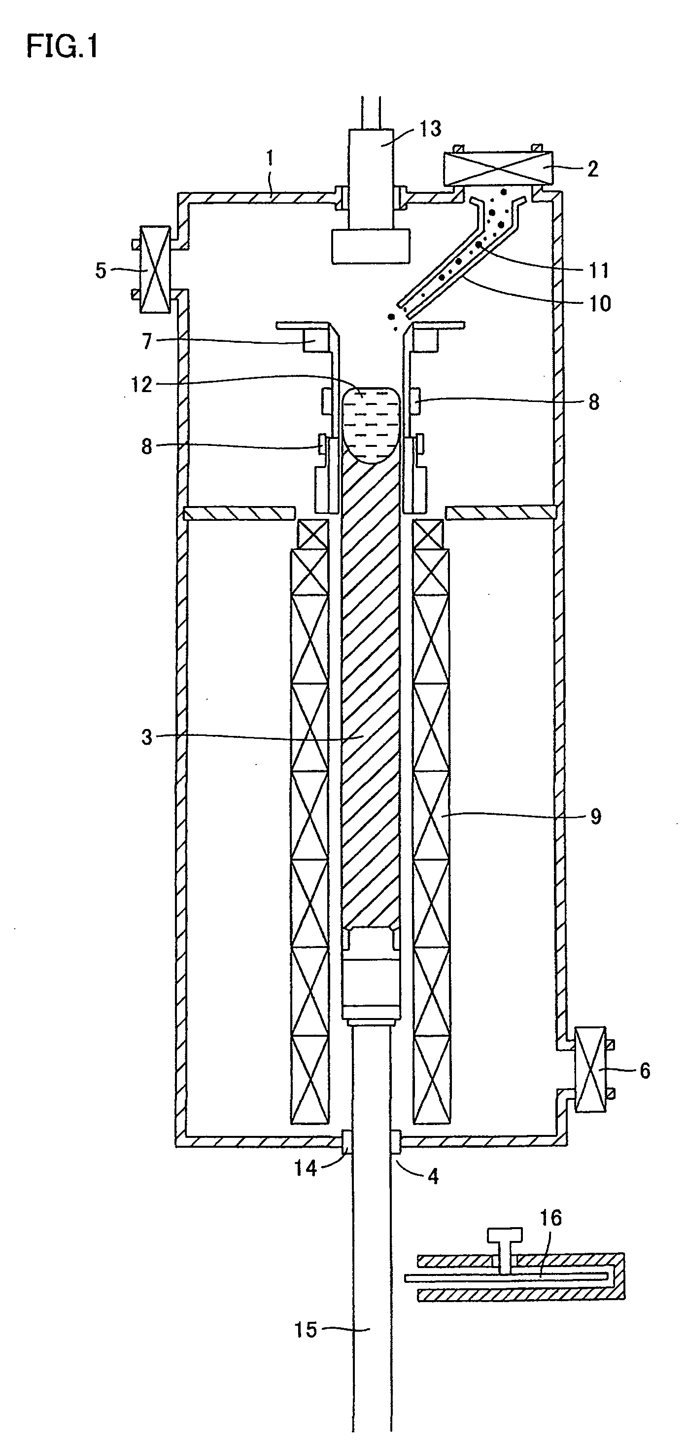
[0057]To ascertain the effects of the present invention, we have cast polycrystalline silicon and evaluated its conversion efficiency as a solar cell.

[0058]Using an electromagnetic casting furnace shown in the aforementioned FIG. 1, a silicon ingot intended as a source material for a solar cell substrate was cast with a square cross section of 350 mm in side length.

[0059]The comparative examples, Test Nos. T1-T4, were at the time of casting given a current value of 6000 A and a frequency of 12 kHz for the alternating current applied on the induction coil. Moreover, Test No. T5, an inventive example of the present invention, was given a current value of 4500 A and a frequency of 25 kHz for the alternating current applied on the induction coil, while Test Nos. T6-T8, inventive examples, were given a current value of 4000 A and a frequency of 30 kHz for the alternating current at the time of casting. Apart from the current value and the frequency of the applied alternating current, bot...


PUM

PropertyMeasurementUnit
frequencyaaaaaaaaaa
side lengthaaaaaaaaaa

Abstract

In a casting method for polycrystalline silicon in which a bottomless cooling crucible with a part of a certain length in an axial direction being circumferentially and plurally sectioned is provided inside an induction coil, producing a silicon melt within the cooling crucible by means of electromagnetically induced heating by the induction coil, and withdrawing the silicon melt in a downward direction while being solidified, an alternating current with a frequency of 25-35 kHz is applied on the induction coil. According to the casting method for polycrystalline silicon of the present invention, in addition to preventing rapid cooling of the ingot surface at the time of solidifying the molten silicon and producing the ingot, the stirring of the molten silicon inside the crucible is suppressed to thereby promote the growth of large diameter crystals, with the result that the conversion efficiency of the cast polycrystalline silicon used as solar cells is increased.

Description

BACKGROUND OF THE INVENTION[0001]1. Field of the Invention[0002]The present invention relates to a continuous casting method for polycrystalline silicon by electromagnetic induction. More particularly, it relates to a casting method for polycrystalline silicon in which, at the time of solidifying the molten silicon and producing the ingot, a rapid cooling of the ingot surface is moderated, while allowing the stirring of molten silicon in a crucible to be suppressed to promote the growth of a crystal with a large diameter, thereby enabling to increase a conversion efficiency when used as a solar cell.[0003]2. Description of the Related Art[0004]Silicon crystals are being used as substrate materials for the majority of solar cells presently produced. Silicon crystals are classified as single crystals and polycrystals, but generally speaking, the use of single crystals as substrates proves to be superior in obtaining solar cells with high conversion efficiency when converting incident ...

Claims


Application Information

Patent Timeline
Patent Type & Authority Applications(United States)
IPC IPC(8): C30B9/00
CPCC30B11/001C30B29/06C30B28/06C30B11/003
Inventor SASATANI, KENICHINAKAGAWA, KEITAONIZUKA, TOMOHIROKUBO, NOBUYUKI
Owner SUMCO CORP
Why Eureka
Try Eureka