Nitride semiconductor device and manufacturing method thereof

a semiconductor device and nitride technology, applied in the field of field effect transistors, can solve the problems of limited ohmic contact reduction, and achieve the effect of small serial resistance components

Active Publication Date: 2008-09-11
PANASONIC CORP
View PDF11 Cites 45 Cited by
  • Summary
  • Abstract
  • Description
  • Claims
  • Application Information

AI Technical Summary

Benefits of technology

[0008]In view of the above problems, it is an object of the present invention to provide a nitride semiconductor device with low parasitic resistance by reducing the ohmic contact resistance by lowering the barrier height on the interface of metal and semiconductor.
[0031]Since the same number of group-III atoms and group-V atoms are arranged on the same plane on the non-polar surface such as (11-20) plane, (1-100) plane, (03-38) plane or (03-316) plane in plane direction, the spontaneous polarization at the contact surface with the ohmic electrode only generates in the horizontal direction of the contact surface but not in the vertical direction. In the same manner, piezoelectric polarization does not generate in the vertical direction. Therefore, polarized electric charge does not generate on the surface of non-polar surfaces, and the barrier height at the interface of ohmic electrode and nitride semiconductor layer is reduced compared to a case where an ohmic electrode is formed on a polar surface such as (0001) plane, and thus the ohmic contact resistance can be reduced.

Problems solved by technology

Thus, even when sintering (thermal treatment) is performed, the barrier height is not fully lowered at the interface of the semiconductor layer and metal, and thus the reduction of ohmic contact is limited.

Method used


Image

  • Nitride semiconductor device and manufacturing method thereof
  • Nitride semiconductor device and manufacturing method thereof
  • Nitride semiconductor device and manufacturing method thereof

Examples


first embodiment

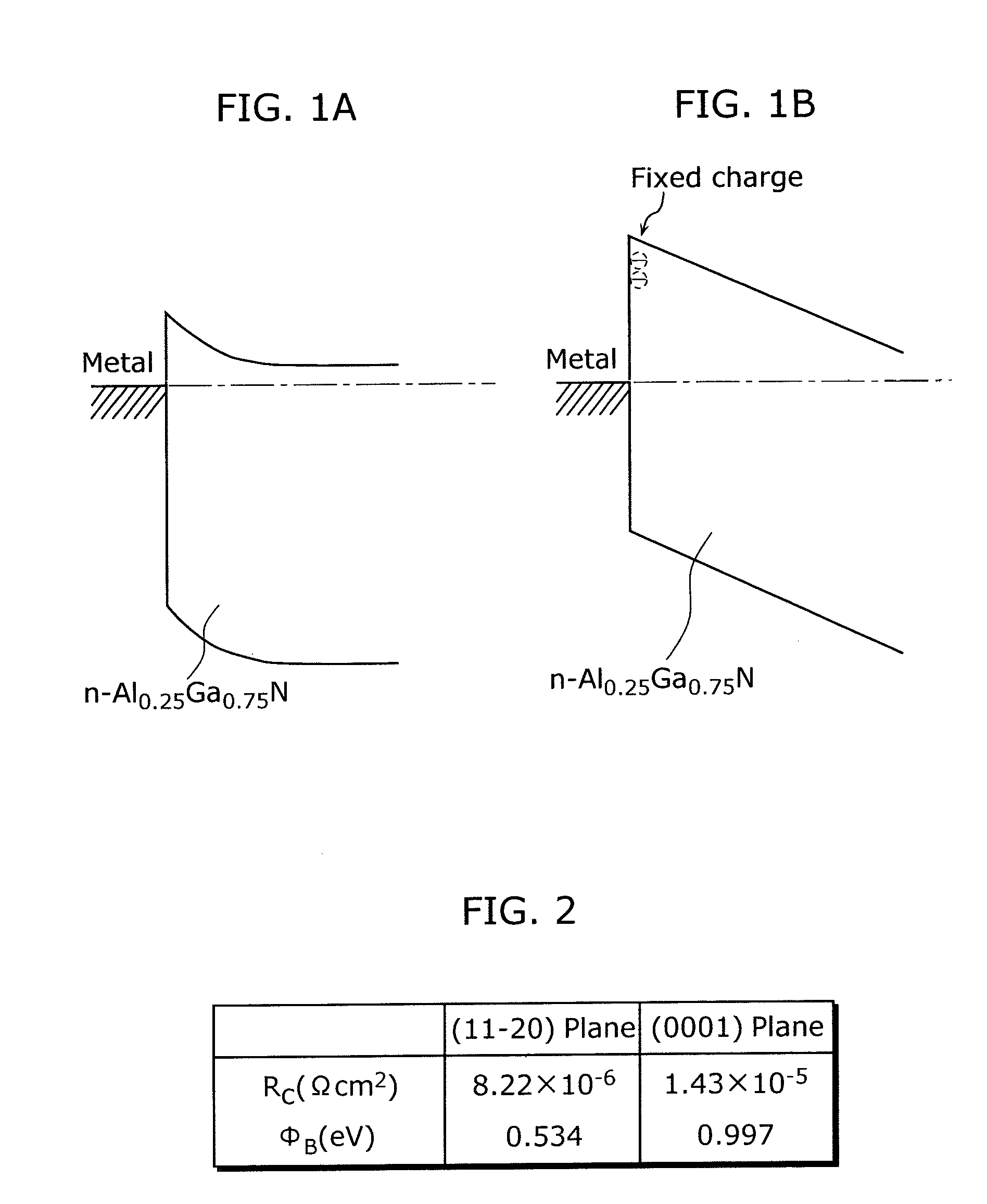
[0057]FIG. 1A is a band diagram of a metal / Al0.25Ga0.75N interface formed on (11-20) plane and FIG. 1B is a band diagram of a metal / Al0.25Ga0.75N interface formed on (0001) plane.

[0058]On the metal / Al0.25Ga0.75N interface formed on (0001) plane, piezoelectric polarization and spontaneous polarization cause polarized charge as shown in FIG. 1B, resulting in a high barrier at the metal / semiconductor interface. On the contrary, on the metal / Al0.25Ga0.75N interface on the (11-20) plane, since polarization electric field is not generated, which lower the barrier height on the metal and semiconductor interface. Here, the following equation (1) represents a contact resistance RC on the metal and semiconductor interface.

RC=kqA*Texp(qΦBnkT)Equation(1)

[0059]In the equation (1), k denotes Boltzmann constant, q denotes elementary charge, A* denotes Richardson constant, T denotes temperature, and φBn denotes the barrier height at the interface of AlGaN and the gate electrode. The equation indica...

second embodiment

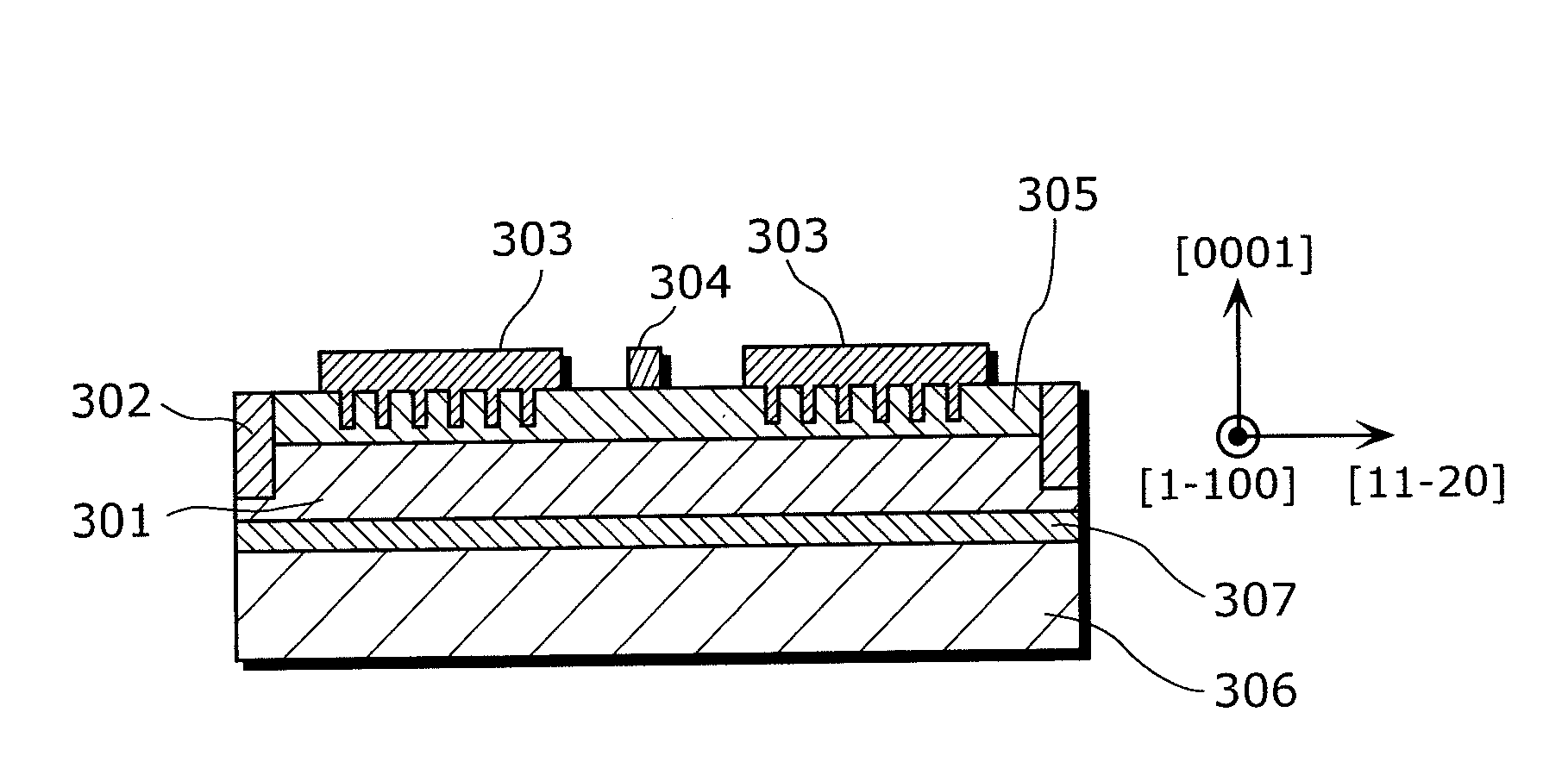
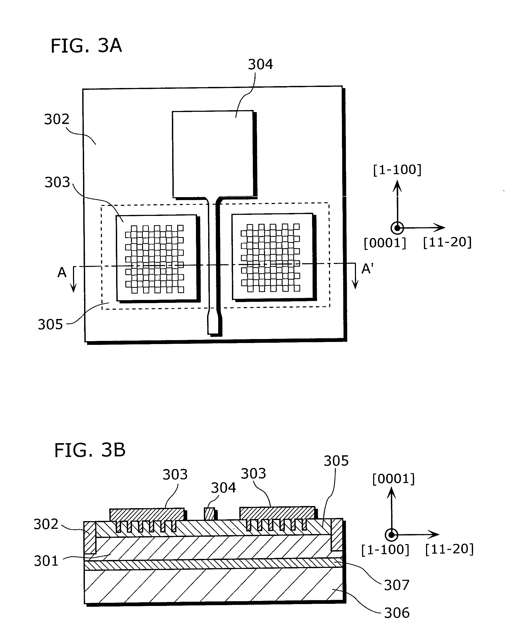
[0089]FIG. 8A is a top view of the HFET according to the second embodiment of the present invention, and FIG. 8B is a cross-sectional view of the HFET (a cross-sectional view at line AA′ in FIG. 8A).

[0090]The HFET includes a GaN layer 801, a device isolation layer 802, an ohmic electrode 803, an n-type cap layer 804, a gate electrode 805, an n-type Al0.25Ga0.75N layer 806, a sapphire substrate 807 and a buffer layer 808. Note that, the cap layer 804 is an example of the first semiconductor layer according to the present embodiment, or stated differently, the low resistance cap layer. In addition, the GaN layer 801 is an example of the third semiconductor layer according to the present invention.

[0091]In the HFET, the undoped GaN layer 801 with the layer thickness of 2 μm is formed on the sapphire substrate 807 having (0001) plane as the main surface via the buffer layer 808, and the n-type Al0.25Ga0.75N layer 806 with the thickness of 25 nm is formed thereon. On the n-type Al0.25Ga0...

third embodiment

[0103]FIG. 9A is a top view of the HFET according to the third embodiment, and FIG. 9B is a cross-sectional view (a cross-sectional view at the line AA′ in FIG. 9A) of the HFET.

[0104]The HFET includes a GaN layer 901, a device isolation layer 902, an ohmic electrode 903, a gate electrode 904, a first n-type Al0.25Ga0.75N layer 905, a second n-type Al0.25Ga0.75N layer 906, a sapphire substrate 907 and a buffer layer 908.Note that the GaN layer 901 is an example of the third semiconductor layer according to the present invention. In addition, the first n-type Al0.25Ga0.75N layer 905 and the second n-type Al0.25Ga0.75N layer 906 are respectively an example of the first nitride semiconductor layer and the second nitride semiconductor layer of the present invention.

[0105]In the HFET, the undoped GaN layer 901 with the thickness of 2 μm is formed on the sapphire substrate 907 having (0001) plane as the main surface via the buffer layer 908, the n-type Al0.25Ga0.75N layer 905 with the thic...


PUM

PropertyMeasurementUnit
gate lengthaaaaaaaaaa
thicknessaaaaaaaaaa

Abstract

It is an object of the present invention to provide a nitride semiconductor device with low parasitic resistance by lowering barrier height to reduce contact resistance at an interface of semiconductor and metal. The nitride semiconductor device includes a GaN layer, a device isolation layer, an ohmic electrode, an n-type Al0.25Ga0.75N layer, a sapphire substrate, and a buffer layer. A main surface of the n-type Al0.25Ga0.75N layer is on (0001) plane as a main surface, and concaves are arranged in a checkerboard pattern on the surface. The ohmic electrode contacts the sides of the concaves of the n-type Al0.25Ga0.75N layer, and the sides of the concaves are on non-polar surfaces such as (11-20) plane or (1-100) plane.

Description

BACKGROUND OF THE INVENTION[0001](1) Field of the Invention[0002]The present invention relates to a field effect transistor made of high breakdown voltage nitride semiconductor having high frequency and the manufacturing method thereof.[0003](2) Description of the Related Art[0004]Group-III nitride semiconductors such as GaN have advantageous properties such as large bandgap, large dielectric strength, and high saturated drift velocities of electrons, and are expected to be applied to high frequency and high output devices. Furthermore, in an AlGaN / GaN heterojunction, highly concentrated two-dimensional electron gas (2DEG) at approximately 1×1013 cm−2 is generated on a heterojunction interface due to spontaneous polarization and piezoelectric polarization. Electric devices such as a Field Effect Transistor (FET) and a Schottky Barrier Diode (SBD) made of the nitride semiconductors are actively developed using these properties.[0005]In order to improve the properties of the Group-III...

Claims


Application Information

Patent Timeline
Patent Type & Authority Applications(United States)
IPC IPC(8): H01L29/778H01L21/205
CPCH01L29/045H01L29/2003H01L29/7787H01L29/41766H01L29/66462H01L29/4175
Inventor KURODA, MASAYUKIUEDA, TETSUZO
Owner PANASONIC CORP
Why Eureka
Try Eureka