High throughput brightfield/darkfield water inspection system using advanced optical techniques

a brightfield/darkfield wafer and inspection system technology, applied in the field of optical inspection of semiconductor wafers, can solve the problems of low background return, difficult detection of particles, low detection efficiency, etc., and achieve the effect of greater detection levels

Inactive Publication Date: 2008-09-18
KLA CORP
View PDF20 Cites 15 Cited by
  • Summary
  • Abstract
  • Description
  • Claims
  • Application Information

AI Technical Summary

Benefits of technology

[0037]The brightfield beamsplitter provided is removable, and preferably replaced with a blank, or glass, when performing darkfield illumination. This allows more light to pass to sensor and permits greater levels of detection in darkfield imaging. An alternative method for producing the same result is to perform brightfield imaging in a selected color light spectrum and performing darkfield in a different frequency light spectrum, such as red being selected for brightfield illumination and green for darkfield illumination.

Problems solved by technology

The small reduction in returned energy resulting from the small particle makes the particle difficult to detect.
Further, the small reduction in energy from a small particles often masked out by reflectivity variations from the bright surrounding background such that small particles cannot be detected without numerous false detections.
Additionally, if the small particle is on an area of low reflectivity, which may occur for some process layers on wafers and always for reticles, photomasks, and flat panel displays, the resultant background return is low and any further reduction due to the presence of a particle becomes very difficult to detect.
However, while this assumption permits a thorough inspection for particles on blank and unpatterned specimens, in the presence of circuit features a darkfield particle inspection system can only detect large particles which protrude above the circuit features.
The resulting detection sensitivity is not satisfactory for advanced VLSI circuit production.
While some attempts to improve darkfield performance have been attempted, such systems tend to have drawbacks, including drawbacks resulting from the very nature of darkfield illumination.
Due to the nature of lasers, the application of light in darkfield illumination tends to be non-uniform and limits the amount of data which can be collected in a particular time period.
Further, a system employing a combination of a monochromatic darkfield and a monochromatic brightfield imaging for wafer inspection is poorly adapted for inspecting Chemical Mechanaical Planarized (CMP) wafers, which often have film thickness variations and a grainy texture.
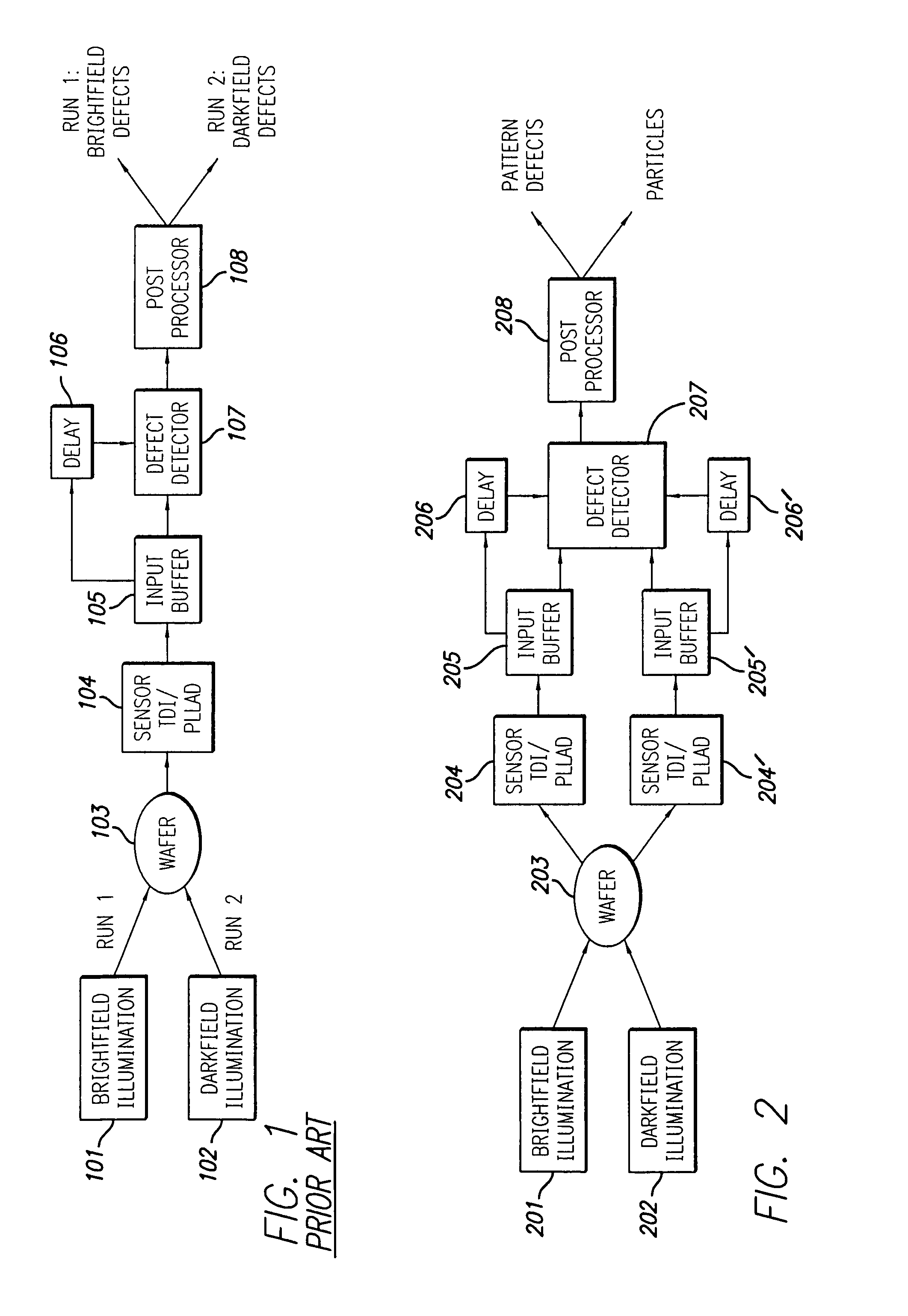
The problem with this mechanization is that throughput, or the time to process a single wafer, is generally poor, and it does not have the capability to use the combined results from both brightfield and darkfield imaging.
The result of this second run is a list of darkfield defects.
This does not completely account for the benefits associated with the combined effects of using brightfield and darkfield, and the amount of time necessary to perform all processing for a single wafer can be significant.
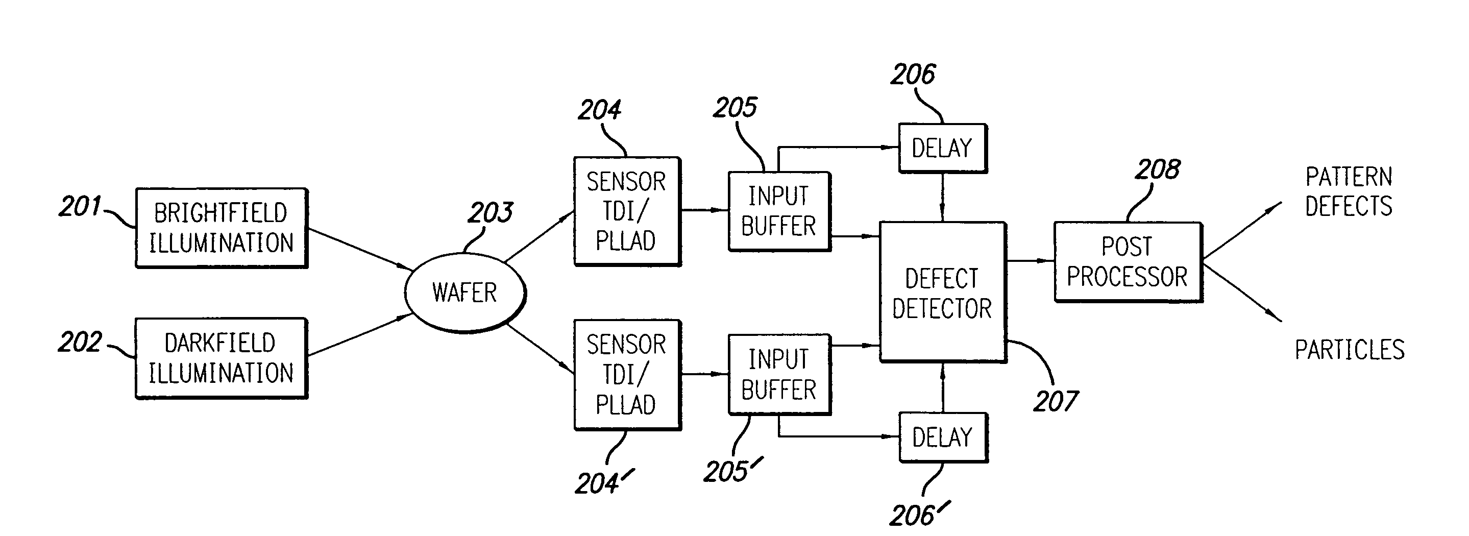
The drawback in implementing the system illustrated in FIG. 2 is that individual TDI and PLLAD sensors 204 and 204′, input buffers 205 and 205′, and delays 206 and 206′ are highly sophisticated and expensive components, and the use of two of each such components significantly increases the cost of the entire machine.
Further, performance of defect detector 207 and post processor 208 requires that all data be available and be evaluated at one time, which can cause significant delays and high processing costs.
This system also uses monochromatic or narrowband brightfield imaging, which has a tendency to exhibit undesirable contrast variations and coherent noise problems as discussed above.
The major limitation of spatial filtering is that only areas having repeating areas or blank areas may be inspected.
There has been little interest in combining brightfield and darkfield techniques due to a lack of understanding of the advantages presented by such a technique.
Microscopes exist on the market today which combine both monochromatic brightfield and darkfield illumination, and such microscopes have a single light source and provide both illuminations simultaneously, thus making it impossible to separate the brightfield and darkfield results.
A further limitation of prior systems is that the illumination sources tend to be fixed in place, which also fixes the ability of the system to pick up defects in surfaces or specimens having different physical properties.
If the specimen contains an irregular surface configuration, such as excess material or a semiconductor pattern, the fixed angle of the light source may not optimally scatter the applied light, inhibiting the ability to detect defects.
Also, the support mechanisms and circuitry associated with the light source tend to be large and bulky, thereby impeding the repositioning capability of the light source.
Another problem with brightfield / darkfield imaging is the use of imaging devices within the same physical space.
However, due to the optical, physical, and other characteristics of components used in brightfield / darkfield imaging, some components tend to provide advantages with one form of illumination and disadvantages for the other illumination scheme.
Another problem associated with wafer inspection systems is the control of light level.
Control of light level is particularly complex and critical where a high level of light collection efficiency is desired, and where the gain of the detector is not readily controlled.
These systems either do not perform sufficiently and / or are too costly or complex to use efficiently.

Method used


Image

  • High throughput brightfield/darkfield water inspection system using advanced optical techniques
  • High throughput brightfield/darkfield water inspection system using advanced optical techniques
  • High throughput brightfield/darkfield water inspection system using advanced optical techniques

Examples


Embodiment Construction

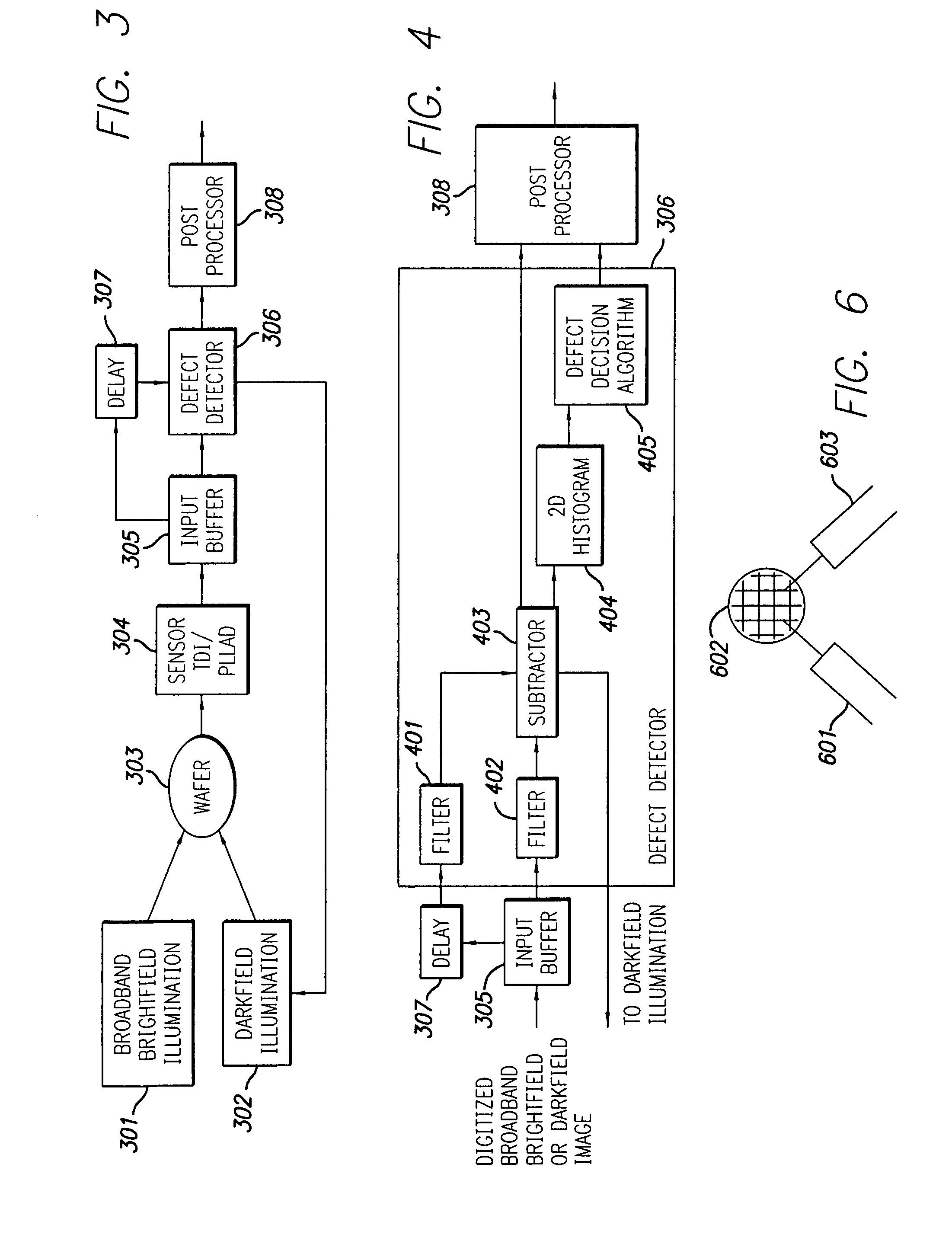
[0055]The inventive system herein combines large pixel DDF (Directional Dark Field) illumination with broadband brightfield illumination to enable increased sensitivity to previous brightfield systems at higher throughput with reduced image computing power. The system includes a dual darkfield illumination module, providing two laser illumination beams having adjustable grazing angle, light level, and polarization.

[0056]Darkfield imaging collects scattered light from a defect, while brightfield imaging collects reflected light. At a given pixel size, a very small (sub-pixel) imaging system averages everything seen in the pixel, including defect plus background. Brightfield imaging uses a small enough pixel to resolve the edges of the defect and thereby detect a contrast. Darkfield imaging averages everything contained in a pixel, but the background is always black, and even small defects have a tendency to scatter large amounts of light. A flat, opaque defect may scatter very little...


PUM

PropertyMeasurementUnit
angleaaaaaaaaaa
azimuth angleaaaaaaaaaa

Abstract

The broadband brightfield / darkfield wafer inspection system provided receives broadband brightfield illumination information via a defect detector, which signals for initiation of darkfield illumination. The defect detector forms a two dimensional histogram of the defect data and a dual mode defect decision algorithm and post processor assess defects. Darkfield radiation is provided by two adjustable height laser beams which illuminate the surface of the wafer from approximately 6 to 39 degrees. Each laser is oriented at an azimuth angle 45 degrees from the orientation of the manhattan geometry on the wafer, and 90 degrees in azimuth from one another. Vertical angular adjustability is provided by modifying cylindrical lens position to compensate for angular mirror change by translating an adjustable mirror, positioning the illumination spot into the sensor field of view, rotating and subsequently moving the cylindrical lens. A brightfield beamsplitter in the system is removable, and preferably replaced with a blank when performing darkfield illumination. Light level control for the system is provided by a dual polarizer first stage. Light exiting from the second polarizer passes through a filter which absorbs a portion of the light and comprises the second stage of light control. The beam then passes through a polarizing beamsplitter. The second channel is further reflected and polarized and both beams thereafter illuminate the substrate.

Description

[0001]This application is a continuation-in-part of U.S. patent application Ser. No. 08 / 884,467, entitled “Optical Inspection of a Specimen Using Multi-Channel Responses from the Specimen,” filed on Jun. 27, 1997, which is a continuation of U.S. patent application Ser. No. 08 / 489,019, filed on Jun. 6, 1995, now abandoned.BACKGROUND OF THE INVENTION[0002]1. Field of the Invention[0003]The present invention relates generally to the art of optical inspection of semiconductor wafers, and more specifically to a high throughput brightfield and darkfield wafer inspection system having image processing redirected from the mechanical and electronics segments of the inspection system to the optical domain.[0004]2. Description of the Related Art[0005]Semiconductor wafer inspection techniques have historically utilized brightfield illumination, darkfield illumination, or spatial filtering. Brightfield imaging is not generally sensitive to small particles. Brightfield imaging tends to scatter sm...

Claims


Application Information

Patent Timeline
Patent Type & Authority Applications(United States)
IPC IPC(8): G01N21/55G01N21/88G01N21/95G01N21/956
CPCG01N21/8806G01N2021/8825G01N21/95607G01N21/9501
Inventor FAIRLEY, CHRISTOPHER R.FU, TAO YIPERELMAN, GERSHONTSAI, BIN-MING BENJAMIN
Owner KLA CORP
Why Eureka
Try Eureka