Pixel Structure For A Solid State Light Emitting Device

a light emitting device and solid-state technology, applied in solid-state devices, electric lighting sources, light sources, etc., can solve the problems of inability to position individual light emitting elements within five millimeters of each other, inability to provide a contiguous illuminated area, inherent limitations on the brightness per unit area, etc., to maximize current flow and minimize current injection

Inactive Publication Date: 2008-10-09
KIRSTEEN MGMT GRP
View PDF12 Cites 12 Cited by
  • Summary
  • Abstract
  • Description
  • Claims
  • Application Information

AI Technical Summary

Benefits of technology

[0021]a field oxide region below the electrical contact to minimize current injection below the electrical contact, thereby maximizing current flow in active layer structure adjacent to the metal electrical contact.

Problems solved by technology

Unfortunately, conventional shaped light emitting devices must be constructed from a number of individual light emitting elements, such as LEDs, which typically cannot be constructed with an area greater than about four mm2 due to inherent limitations in compound semiconductor processing technologies, e.g. a lattice mismatch between substrate and active layers.
Moreover, the individual light emitting elements typically cannot be positioned within five millimeters of each other, because of the need to provide physical mounting, optical coupling and electrical interconnection for each of the individual elements.
Accordingly, the emissive shapes constructed do not provide a contiguous illuminated area, and have inherent limitations on the available brightness per unit area.
Furthermore, the refinement or smoothness of the shape is limited by the granularity of the individual lighting elements, and the light emitting elements cannot be made smaller than a certain size because of the physical constraints in their mounting and interconnection.
ITO may be susceptible to damage from high electric fields of approximately 1 MV / cm, which is believed may lead to the decomposition of In2O3 and SnO2.
The work function locally in this region would be reduced to approximately 4.4 eV and 4.2 eV for indium and tin, respectively, which would result in a significant increase in the electron injection characteristics of the ITO layer 4 and the formation of hot spots due to local current hogging potentially leading to device destruction.
All of these effects serve to modify, and in some instances increase, the internal electric field in the vicinity of the contact interfaces with the active layer 3, which will lead to an early breakdown and destruction of the light emitting device 1.

Method used


Image

  • Pixel Structure For A Solid State Light Emitting Device
  • Pixel Structure For A Solid State Light Emitting Device
  • Pixel Structure For A Solid State Light Emitting Device

Examples


example process

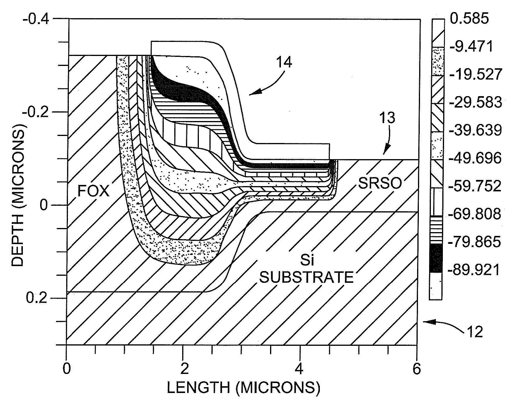
[0057]With reference to FIGS. 6 to 18, the manufacturing process according to the present invention begins with the substrate 23 (FIG. 6). Pad oxide layers 41a and 41b, approximately 500 Angstroms thick, are thermally grown on opposite sides of the substrate 23 by dry oxygen thermal oxidation to protect the substrate during subsequent steps, e.g. to electrically isolate metal contacts from the substrate 23 (FIG. 7a). Nitride layers 42a and 42b, e.g. silicon nitride, approximately 900 Angstroms thick, are deposited over the pad oxide layers 41a and 41b by a suitable deposition technique, e.g. LPCVD (FIG. 7b).

[0058]In FIG. 8, the top nitride layer 42a is patterned on opposite sides thereof and plasma etched down to the pad oxide layer 41a leaving only a central strip. The field oxide regions 21 are grown in the opened areas on opposite sides of the central strip of the pad oxide layer 41a. Preferably, 1 μm of the thermal oxide making up the field oxide regions 21 are grown using a pyr...


PUM


Abstract

A light emitting device includes an active layer structure, which has one or more active layers with luminescent centers, e.g. a wide bandgap material with semiconductor nano-particles, deposited on a substrate. For the practical extraction of light from the active layer structure, a transparent electrode is disposed over the active layer structure and a base electrode is placed under the substrate. Transition layers, having a higher conductivity than a top layer of the active layer structure, are formed at contact regions between the upper transparent electrode and the active layer structure, and between the active layer structure and the substrate. Accordingly the high field regions associated with the active layer structure are moved back and away from contact regions, thereby reducing the electric field necessary to generate a desired current to flow between the transparent electrode, the active layer structure and the substrate, and reducing associated deleterious effects of larger electric fields.

Description

CROSS-REFERENCE TO RELATED APPLICATIONS[0001]The present invention is a continuation-in-part of U.S. patent application Ser. No. 11 / 642,813, filed Dec. 21, 2006 which claims priority from U.S. Patent Application No. 60 / 754,185 filed Dec. 28, 2005, which are incorporated herein by reference.TECHNICAL FIELD[0002]The present invention relates to light emitting devices, and in particular to pixel structures for light emitting devices providing practical solid state light emitting devices.BACKGROUND OF THE INVENTION[0003]To build lighting systems for illumination and projection, there are significant advantages to being able to tailor the shape of the light source, since the shape of the light source and the optical components of the system provide the means to precisely shape the resulting light beam. The shape of the resulting light beam is an important aspect of the lighting system, especially in the creation of solid-state headlamps for the automotive industry, as disclosed in United...

Claims


Application Information

Patent Timeline
Patent Type & Authority Applications(United States)
IPC IPC(8): H01L33/00
CPCH05B33/22
Inventor CHIK, GEORGEMACELWEE, THOMASCALDER, IAINHILL, E. STEVEN
Owner KIRSTEEN MGMT GRP
Why Eureka
Try Eureka