Device and Method for the Demodulation of Modulated Electric Signals

Active Publication Date: 2008-10-09
AMS SENSORS SINGAPORE PTE LTD
View PDF14 Cites 21 Cited by
  • Summary
  • Abstract
  • Description
  • Claims
  • Application Information

AI Technical Summary

Benefits of technology

[0023]The present invention greatly relaxes the requirements to the semiconductor process technology compared to prior-art mixing devices. Only one single demodulation device is required for the demodulation of the current signal. The device works completely in the charge domain, so that no device-matching problems arise during the demodulation process. The operation in the charge domain also allows very simple and efficient demodulation of modulated currents down to a few picoamperes, such as, e.g., modulated photo-currents, without additional noise contributions from the demodulation stage. The size of the new device is even more reduced as only one gate structure and a nu

Problems solved by technology

The above-mentioned mixer circuits have the disadvantage that several dual-gate transistors are required with additional load resistors, low-pass filters or differential amplifiers, which leads to a relatively complex circuit.
Moreover, the size of the circuits does not allow the implementation as elements in a high-density array, such as, e.g., in the pixel structures of image sensors.
Furthermore, the mixing circuit is n

Method used


Image

  • Device and Method for the Demodulation of Modulated Electric Signals
  • Device and Method for the Demodulation of Modulated Electric Signals
  • Device and Method for the Demodulation of Modulated Electric Signals

Examples


first embodiment

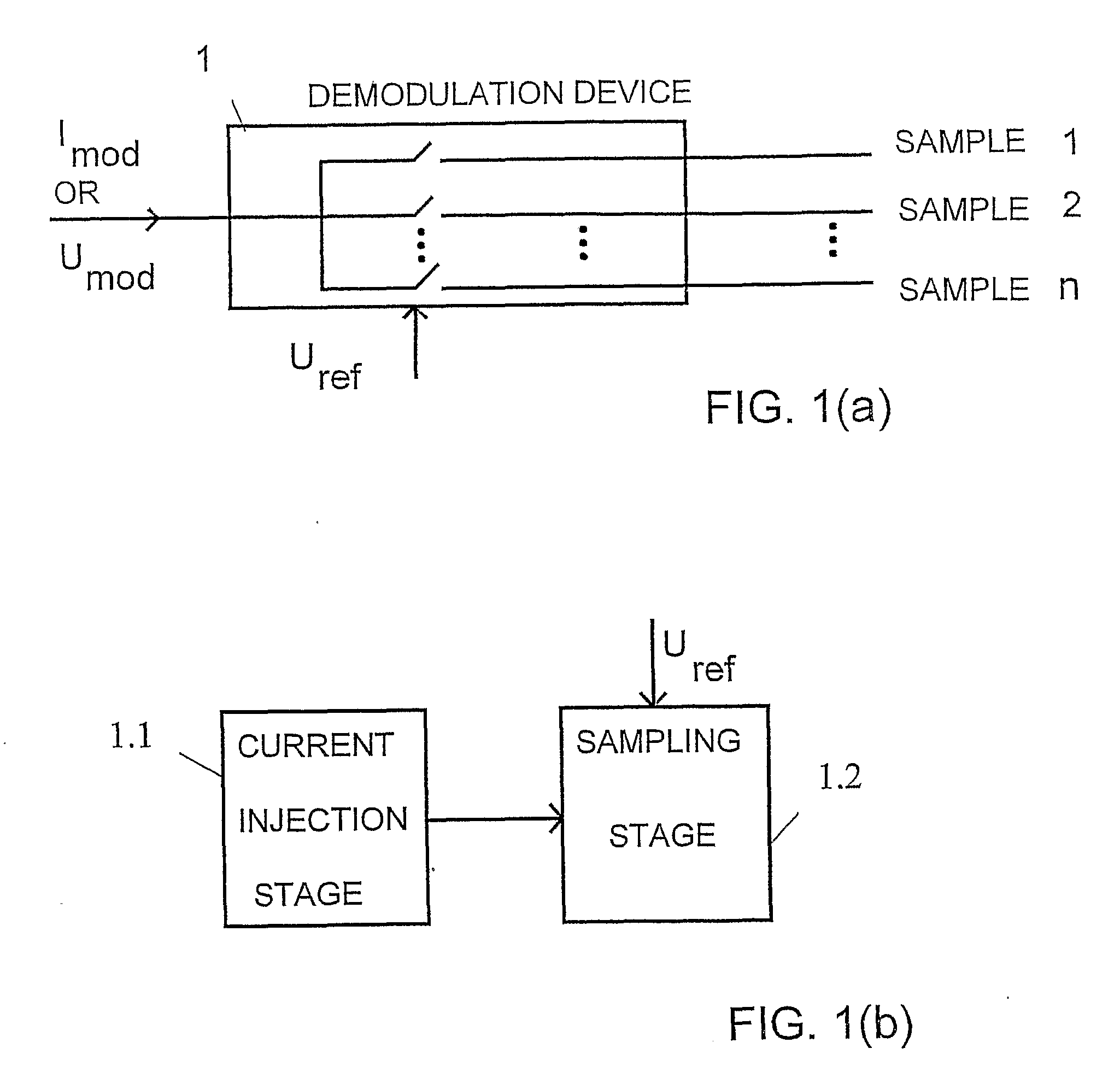
[0050]the sample output stage 1.23 is shown in FIG. 4(a). The sample output stage comprises an accumulation module 1.230 and a charge-voltage converter 1.231. The accumulation module 1.230 is for example a capacitor which integrates the sample current. The integrated charge carriers induce a potential drop over the capacitor that can be read out by a further electronic circuit 1.231. Generally, additional amplification circuits such as e.g. a source follower are foreseen in order to drive the following analogue-to-digital converter circuit or any other electronics not shown in FIG. 4(a).

[0051]The second embodiment of the sample output stage 1.23 is detailed in FIG. 4(b). The sample output stage 1.23 comprises a direct current-voltage converter 1.235 aims at a direct conversion of the sample currents Isample_1, . . . Isample_n into corresponding sample voltages Usample_1, . . . Usample_n. As the accumulation module 1.230 of FIG. 4(a) is not provided in this embodiment, the sample out...

second embodiment

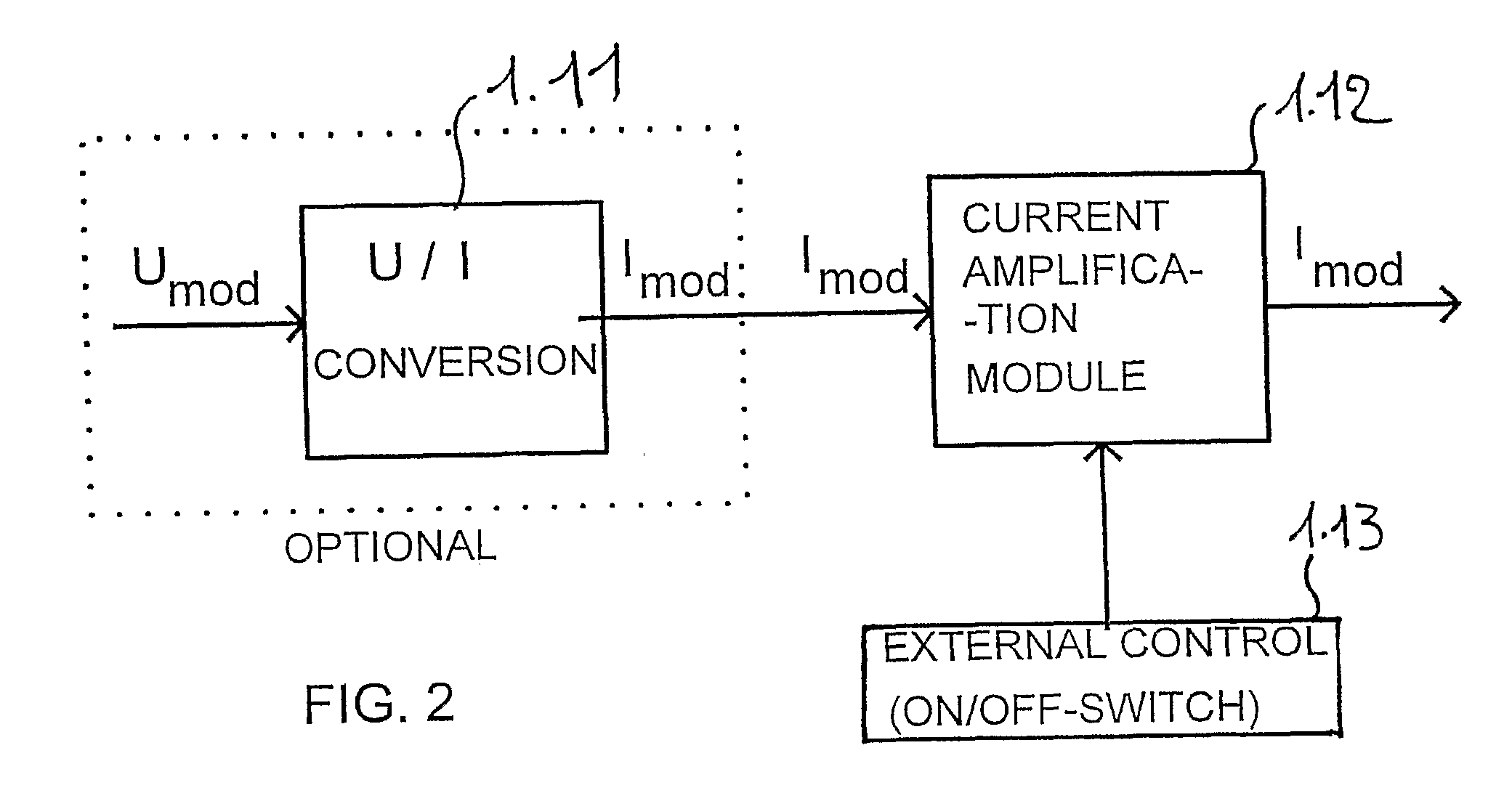
[0064]FIG. 8 shows preferred embodiments of the current-injection stage 1.1 of FIG. 1(b) linked to the sampling stage 1.2 through its injection node IN. In all four FIGS. 8(a)-(d), the modulated current Imod is mirrored using, e.g., the known electronic circuit consisting of two transistors called current mirror. The current Imod is thus amplified using this current-mirror circuit. The mirrored current is used as injection current to the sampling stage 1.2. A switch S controls the duration of current injection into the sampling stage. This switch corresponds to the external control 1.13 of FIG. 2. The switch S can be formed by one single transistor or a transmission gate. FIG. 8(b) illustrates particularly the conversion of the modulated voltage signal Umod into a modulated reference current Iref that is injected into the sampling stage 1.2. The voltage-to-current conversion is done using e.g. a condensator C. FIG. 8(c) illustrates the voltage-to-current conversion Umod into Iref. F...


PUM


Abstract

A demodulation device (1) in semiconductor technology is disclosed. The device (1) is capable of demodulating an injected modulated current. The device (1) comprises an input node (IN1), a sampling stage (DG1, IG1, GS1 IG2, DG2) and at least two output nodes (D1, D2). The sampling stage DG1, IG1, GS1, IG2, DG2) comprises transfer means (GL, GM, GR) for transferring a modulated charge-current signal from the input node (IN1) to one of the output nodes (D1, D2) allocated to the respective time interval within the modulation period. The small size and the ability to reproduce the device (1) in standard semiconductor technologies make possible a cost-efficient integration of the device (1).

Description

FIELD OF THE INVENTION[0001]The present invention relates to a device and a method for the demodulation of all modulated electric signals, e.g., modulated currents or voltages, according to the preambles of the independent claims.[0002]The demodulation method can be exploited in particular for phase-difference measurements of electronic signals and / or for the determination of amplitude and / or intensity. Depending on the particular design and application, the measurement data can be provided in a very short time frame of a few milliseconds or microseconds; even real-time measurements by an instantaneous adaptation of the output signal to the input signals are possible. If the demodulation measurement functions as a reference measurement, the invention allows the demodulation and the acquisition of the user data at the same time.[0003]The device and method according to the invention may be used in many kinds of electronic circuits, mainly with the purpose of signal processing. In part...

Claims


Application Information

Patent Timeline
IPC IPC(8): G02F2/00H03D3/02
CPCH03D7/00
Inventor BUETTGEN, BERNHARDLEHMANN, MICHAELNEUKOM, SIMONOGGIER, THIERRYLUSTENBERGER, FELIX
Owner AMS SENSORS SINGAPORE PTE LTD
Why Eureka
Try Eureka