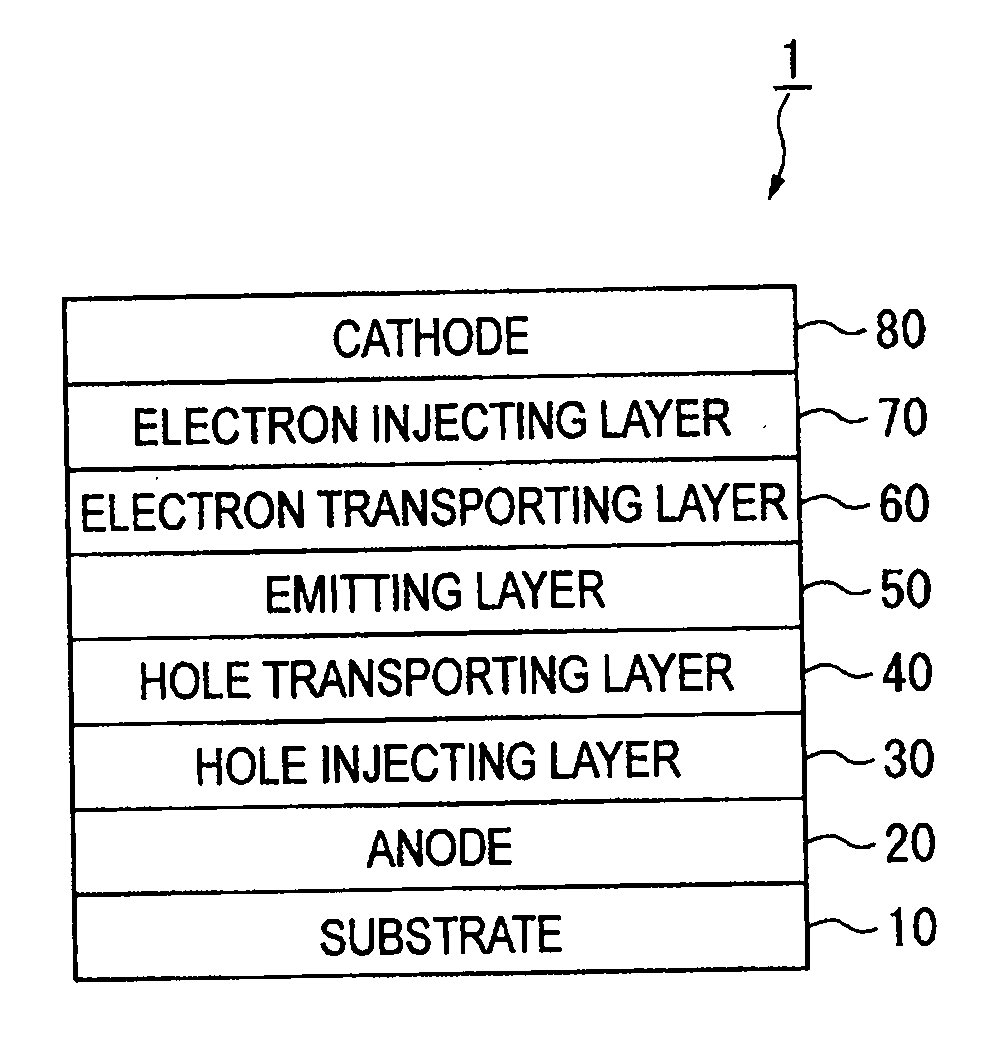
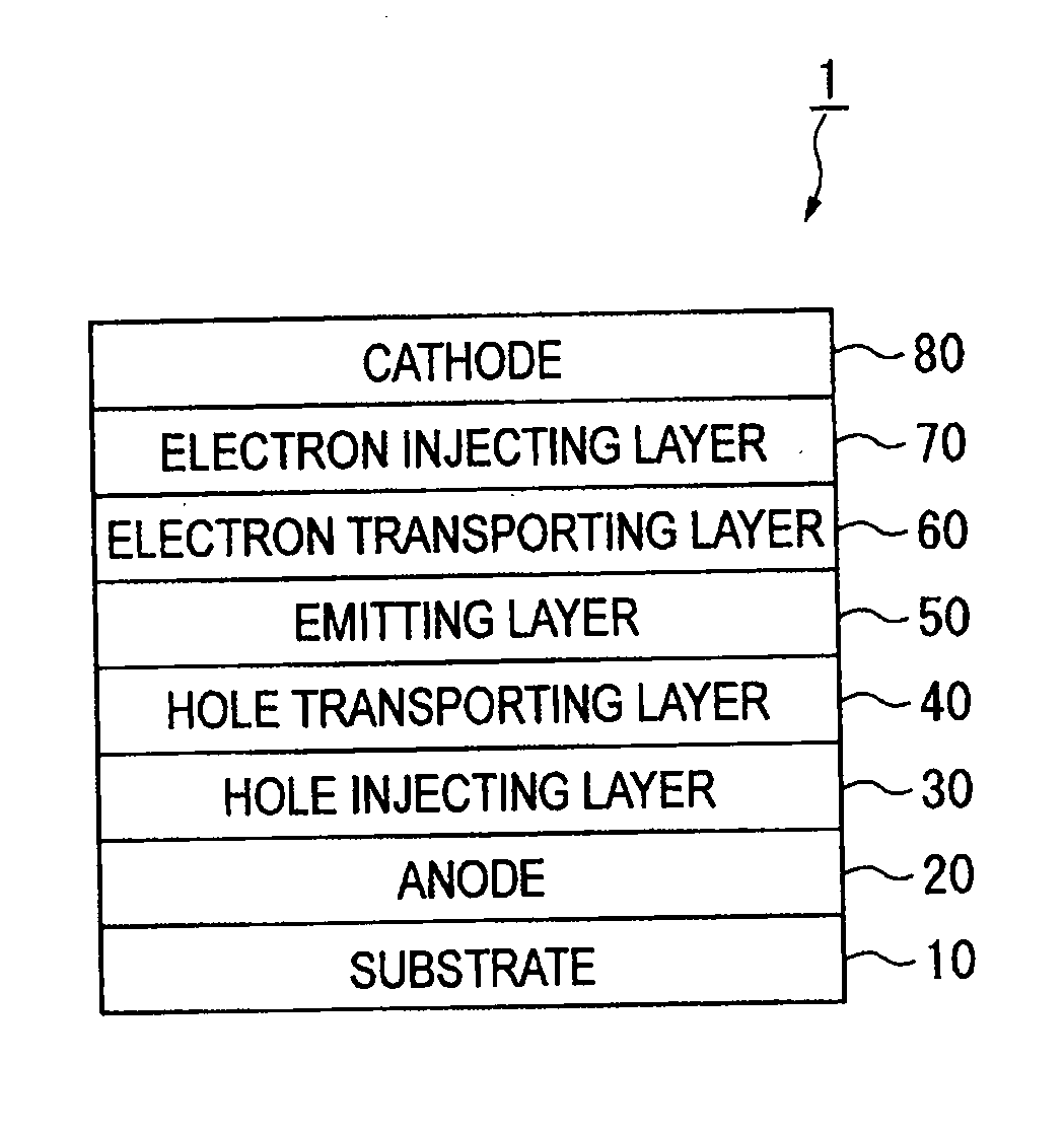
Organic electroluminescence device and display
a technology of electroluminescence device and organic material, which is applied in the direction of luminescent composition, discharge tube luminescnet screen, organic chemistry, etc., can solve the problems of insufficient device performance, inapplicability, and insufficient luminous efficiency and lifetime of such a device, and achieve excellent chromatic purity, long life, and high efficiency
- Summary
- Abstract
- Description
- Claims
- Application Information
AI Technical Summary
Benefits of technology
Problems solved by technology
Method used
Image

Examples
example 1
[0194]A 130 nm-thick transparent electrode formed of indium tin oxide was formed on a glass substrate having a size of 25 mm by 75 mm by 0.7 mm. After the transparent substrate was ultrasonically cleaned in isopropyl alcohol for five minutes, the substrate was further cleaned with UV (ultraviolet) ozone for thirty minutes, and then the substrate was mounted on a vapor deposition apparatus.
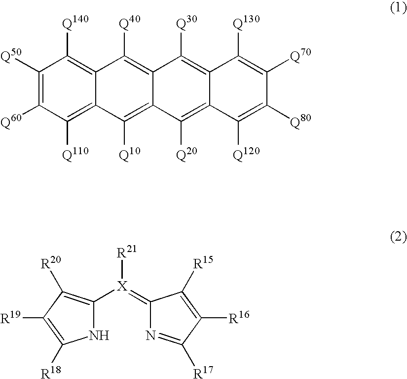
[0195]Initially, N,N′-bis[4-(N,N-diphenylamino)phenyl-1-yl]-N,N′-diphenyl-4,4′-benzidine was deposited on the substrate to form a 60 nm-thick hole injecting layer, and subsequently N,N′-bis[4′-{N-(naphthyl-1-yl)-N-phenyl}aminobiphenyl-4-yl]-N-phenylamine was deposited thereon to form a 10 nm-thick hole transporting layer. Then, the following compound (A-1), a naphthacene derivative, and the following compound (B-1), a compound having a pyrromethene skeleton, were simultaneously deposited thereon by weight ratio of 40 to 0.4 (=0.99 wt %) to form a 40 nm-thick emitting layer.
[0196]Next, the following...
example 2
[0199]An organic EL device was manufactured in the same manner as in Example 1 except that the following compound (A-2) was used in place of the compound (A-1) for forming the emitting layer.
[0200]When a current test was conducted on the obtained device, the organic EL device was driven by a voltage of 4.8 V to emit red light having a luminescence intensity of 720 cd / m2 at a current density of 10 mA / cm2, a trichromatic coordinate of the emitted light was (0.66, 0.33), and efficiency of the device was 7.20 cd / A. In addition, when a continuous direct-current test was conducted with the initial luminescence intensity set at 5,000 cd / m2, time elapsed until the luminescence intensity was reduced by half was 2,000 hours.
example 3
[0201]An organic EL device was manufactured in the same manner as in Example 1 except that the following compound (A-3) was used in place of the compound (A-1) for forming the emitting layer.
[0202]When a current test was conducted on the obtained device, the organic EL device was driven by a voltage of 4.8 V to emit red light having a luminescence intensity of 737 cd / m2 at a current density of 10 mA / cm2, a trichromatic coordinate of the emitted light was (0.66, 0.33), and efficiency of the device was 7.37 cd / A. In addition, when a continuous direct-current test was conducted with the initial luminescence intensity set at 5,000 cd / m2, time elapsed until the luminescence intensity was reduced by half was 3,200 hours.
PUM
| Property | Measurement | Unit |
|---|---|---|
| work function | aaaaa | aaaaa |
| thickness | aaaaa | aaaaa |
| thickness | aaaaa | aaaaa |
Abstract
Description
Claims
Application Information
 - R&D
- Intellectual Property
- Life Sciences
- Materials
- Tech Scout
- Unparalleled Data Quality
- Higher Quality Content
- 60% Fewer Hallucinations
Browse by: Latest US Patents, China's latest patents, Technical Efficacy Thesaurus, Application Domain, Technology Topic, Popular Technical Reports.
© 2025 PatSnap. All rights reserved.Legal|Privacy policy|Modern Slavery Act Transparency Statement|Sitemap|About US| Contact US: help@patsnap.com