System for and Method of Integrating Test Structures into an Integrated Circuit

a test structure and integrated circuit technology, applied in the direction of individual semiconductor device testing, semiconductor/solid-state device testing/measurement, instruments, etc., can solve the problems of inability to provide detailed information, time-consuming and expensive in-line testing, and achieve the effect of affecting cost and highest possible yield

Inactive Publication Date: 2008-10-30
IBM CORP
View PDF10 Cites 14 Cited by
  • Summary
  • Abstract
  • Description
  • Claims
  • Application Information

AI Technical Summary

Benefits of technology

[0009]Based on the issues identified above, what is needed is a means for accurately testing customized circuitry so that adequate feedback can be relayed to the manufacturing line to ensure the highest possible yields. It is a further requirement that t...

Problems solved by technology

The problem with kerf testing is that it does not provide detailed information specific to each die on the wafer and further, cannot provide information about the electrical parameters of certain devices within each of the chips; especially custom designs which have smaller manufacturing lot sizes, device dimensions which vary from standard devices, ...

Method used


Image

  • System for and Method of Integrating Test Structures into an Integrated Circuit
  • System for and Method of Integrating Test Structures into an Integrated Circuit
  • System for and Method of Integrating Test Structures into an Integrated Circuit

Examples


Embodiment Construction

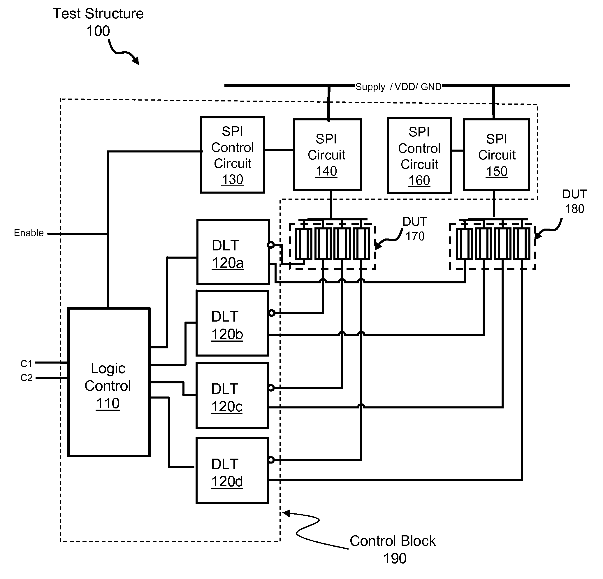
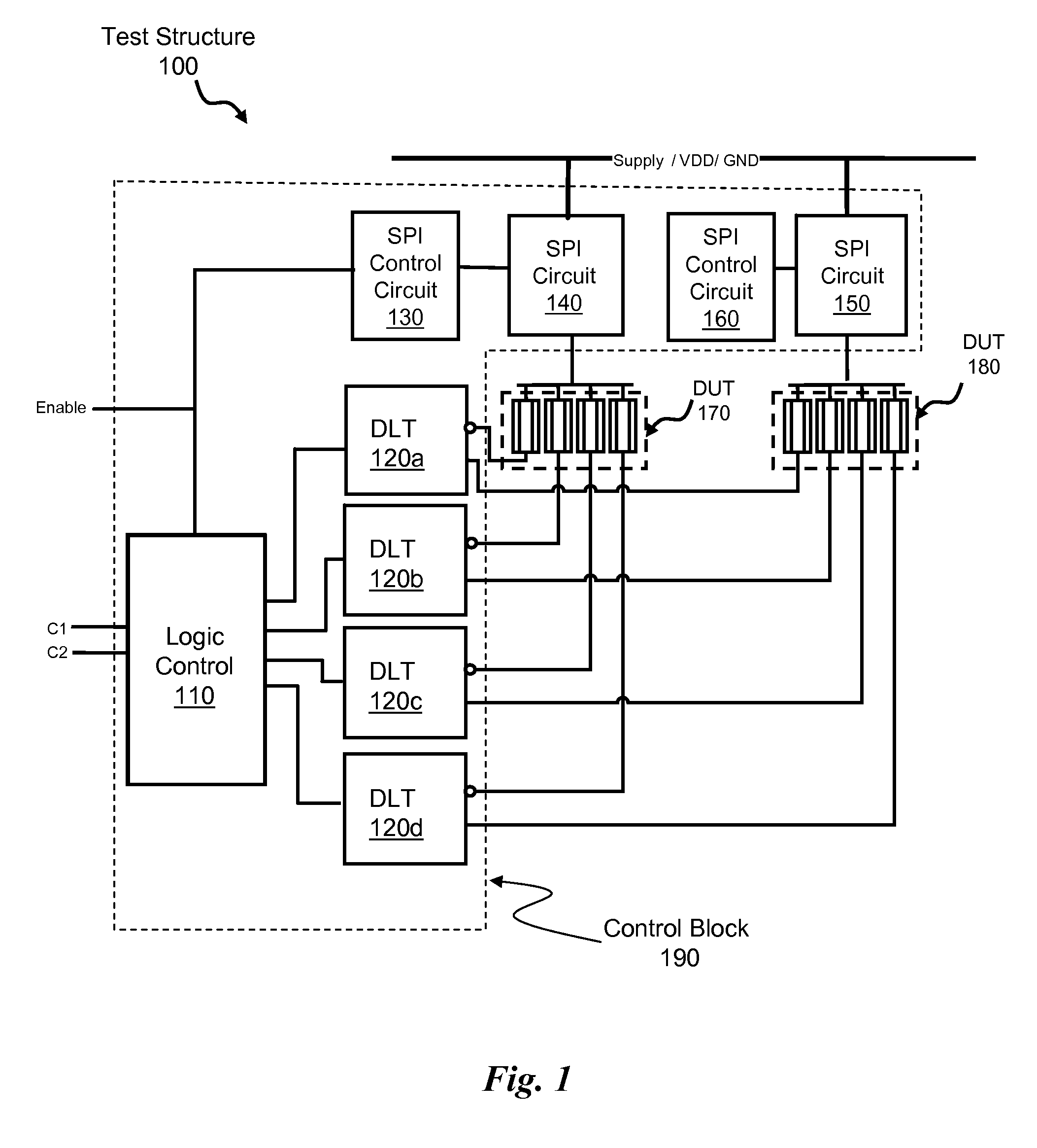
[0040]FIG. 1 shows a test structure 100 of the present invention. Test structure 100 includes a control block 190, which further includes logic control 110, a group of decode level translators (DLT) 120a-d (four DLTs are shown in this example), a pFET SPI circuit 140 coupled to an SPI control circuit 130, and an nFET SPI circuit 150 coupled to SPI control circuit 160. Test structure 100 further includes a DUT 170, which represents one device type (in this example, an array of pFETs) and a DUT 180, which represents a second device type (in this example, an array of nFETs). Each of DUTs 170 and 180 are coupled to control block 190.

[0041]In operation, control block 190 exercises corresponding DUTs 170 and / or 180 and provides resulting test data to a test apparatus (not shown). Each element of test structure 100 is further discussed in the following figures.

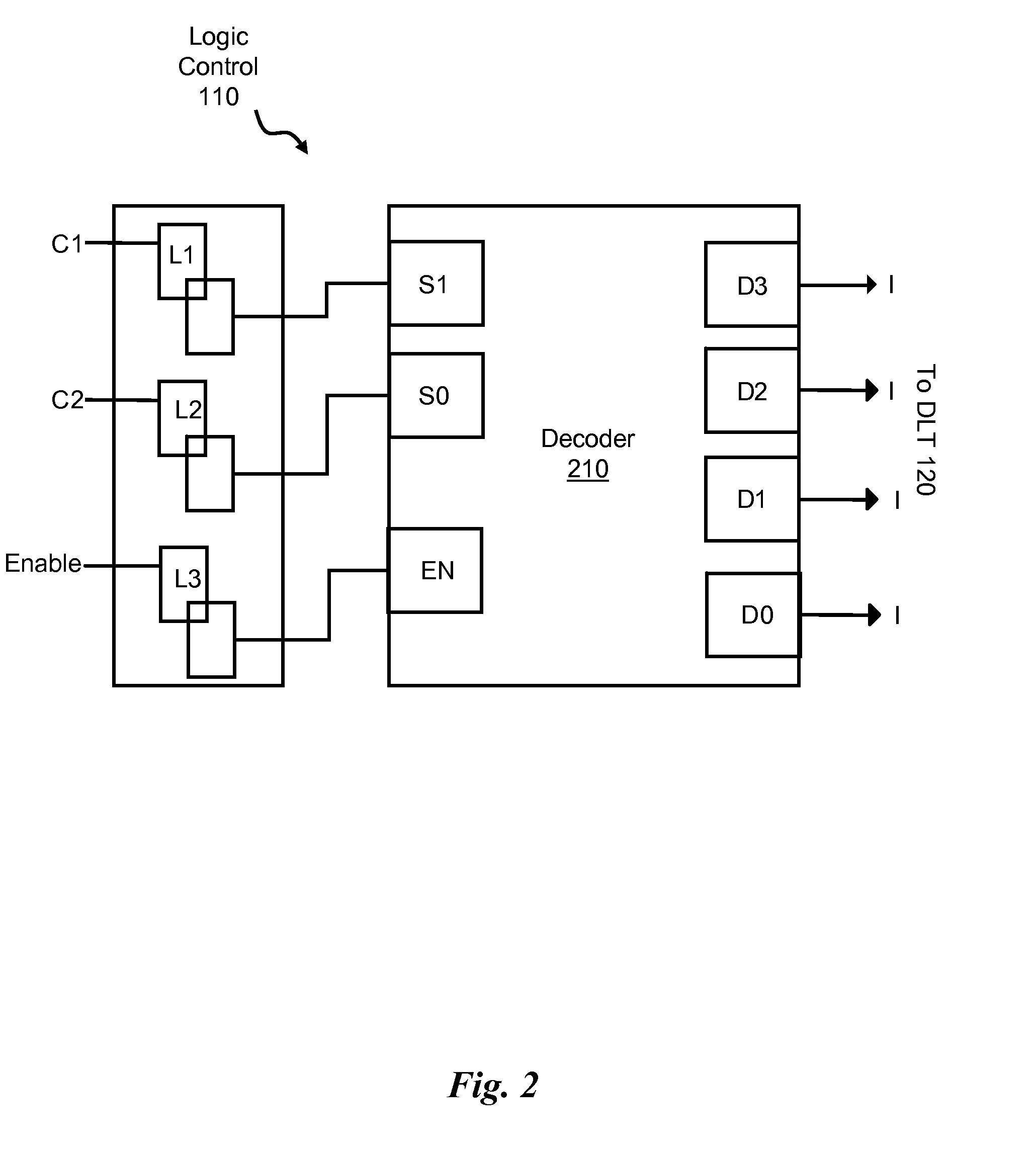
[0042]FIG. 2 shows logic control 110, which includes a control signal C1 coupled to a latch L1, which is further connected to a pad...


PUM


Abstract

A system and method for performing device-specific testing and acquiring parametric data on integrated circuits, for example ASICs, such that each chip is tested individually without excessive test time requirements, additional silicon, or special test equipment. The testing system includes a device test structure integrated into unused backfill space in an IC design which tests a set of dummy devices that are identical to a selected set of devices contained in the IC. The device test structures are selected from a library according to customer requirements and design requirements. The selected test structures are further prioritized and assigned to design elements within the design in order of priority. Placement algorithms use design, layout, and manufacturing requirements to place the selected test structures into the final layout of the design to be manufactured.

Description

CROSS REFERENCES RELATED TO THE APPLICATION[0001]This application is related to pending U.S. application Ser. No. 11 / 459,367 assigned to the present assignee.BACKGROUND OF THE INVENTION[0002]1. Field of the Invention[0003]The invention relates to the field of acquiring manufacturing process data on a part-by-part basis (e.g. chip), and more specifically, to providing a means to acquire device data with which to perform a detailed product analysis, which is further used to tune the manufacturing processes.[0004]2. Background of the Invention[0005]Due to the complex and precise nature of semiconductor manufacturing, it is critical to ensure that all processes in the manufacturing line are within required specifications. This ensures the highest product yield. Monitoring the manufacturing process and correcting for deficiencies is critical for maintaining the health of the line (HOL).[0006]Some testing is done in-line during manufacturing to tune the process real-time, and other tests ...

Claims


Application Information

Patent Timeline
IPC IPC(8): G01R31/00G06F17/50
CPCG01R31/31704G01R31/318364G06F17/5045G06F30/30G01R31/26H01L21/82H01L22/00
Inventor HABIB, NAZMULMCMAHON, ROBERTPERRY, TROY
Owner IBM CORP
Why Eureka
Try Eureka