Semiconductor device and manufacturing method of the same

Inactive Publication Date: 2008-11-20
RENESAS TECH CORP
View PDF0 Cites 16 Cited by
  • Summary
  • Abstract
  • Description
  • Claims
  • Application Information

AI Technical Summary

Benefits of technology

[0016]An object of the present invention is to provide the technology capable of reducing threshold voltage of each of an n channel MOS transistor and a p channel MOS tra

Problems solved by technology

In addition, when different metal materials are used to form gate electrodes of an n channel MOS transistor and a p channel MOS t

Method used


Image

  • Semiconductor device and manufacturing method of the same
  • Semiconductor device and manufacturing method of the same
  • Semiconductor device and manufacturing method of the same

Examples


first embodiment

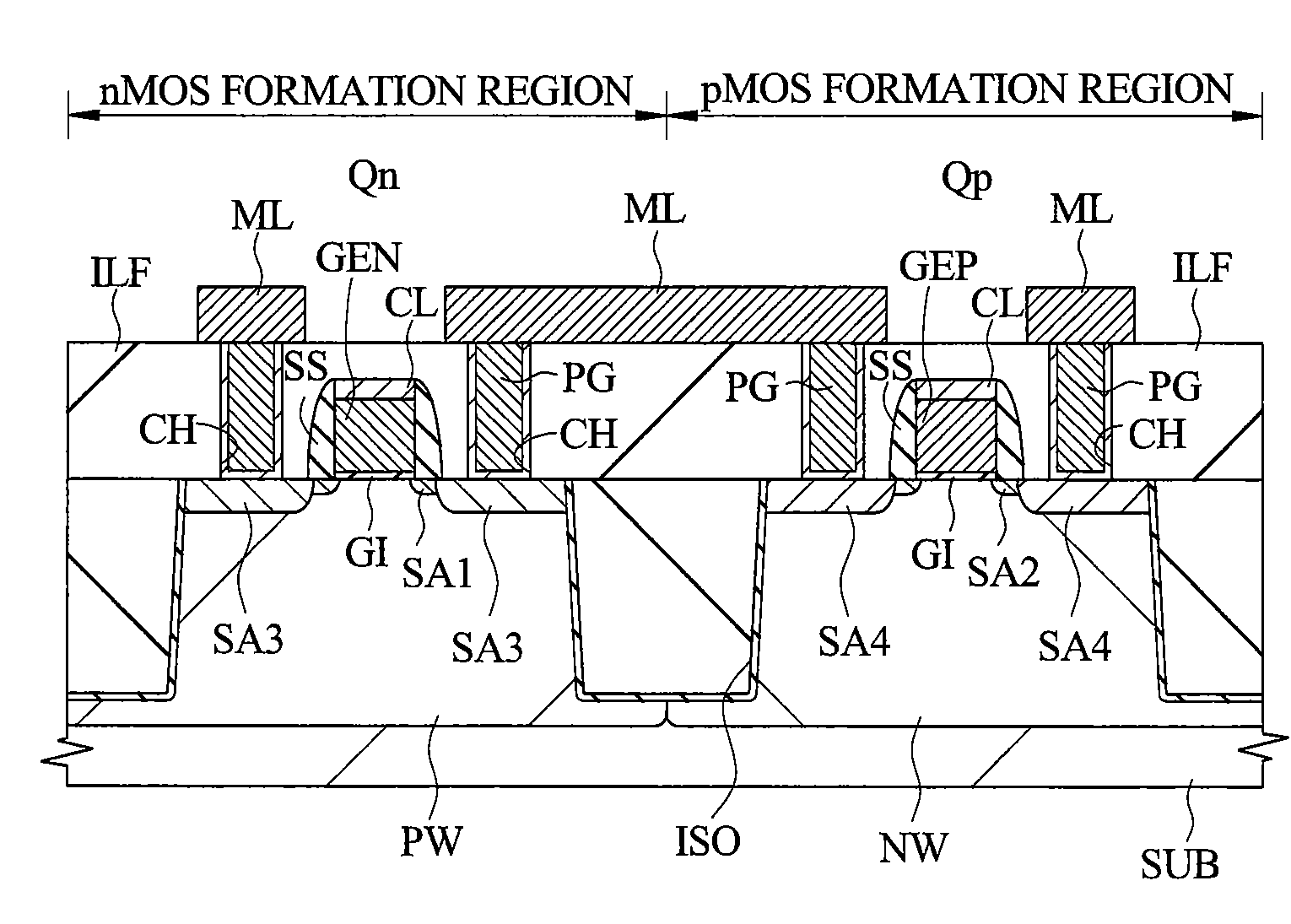
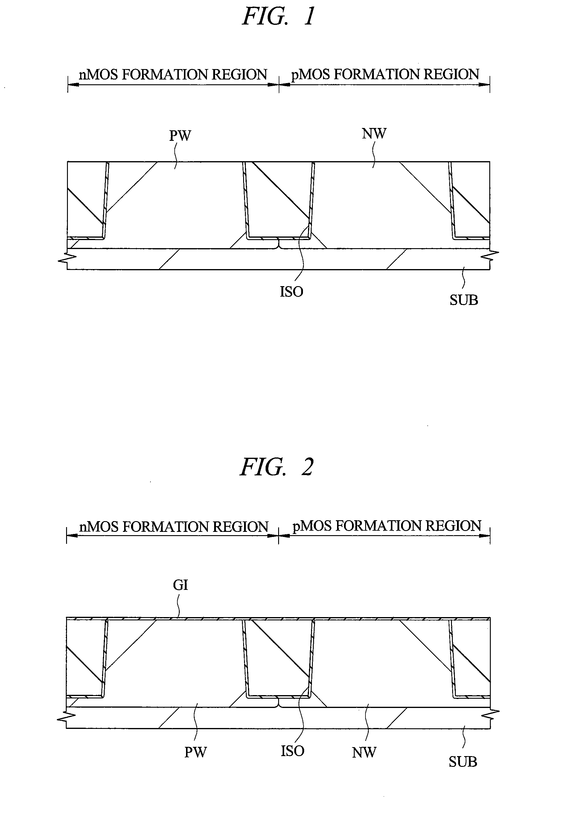
[0051]A manufacturing method of a CMOS (Complementary Metal Oxide Semiconductor) constituted of an n channel MOS transistor and a p channel MOS transistor according to the first embodiment will be described with reference to FIG. 1 to FIG. 10.

[0052]First, as shown in FIG. 1, element isolation trenches ISO are formed using a well-known STI (Shallow Trench Isolation) technology in a main surface (element formation surface) of a semiconductor substrate (hereinafter, referred to as substrate) SUB made of p type single crystal silicon.

[0053]Subsequently, boron is ion-implanted into an n channel MOS transistor formation region (hereinafter, referred to as nMOS formation region, on the left side of the drawing) of the substrate SUB, and phosphorus is ion-implanted into a p channel MOS transistor formation region (hereinafter, referred to as pMOS formation region, on the right side of the drawing). Then, impurity ions for adjusting the threshold voltage of the MOS transistors are implanted ...

second embodiment

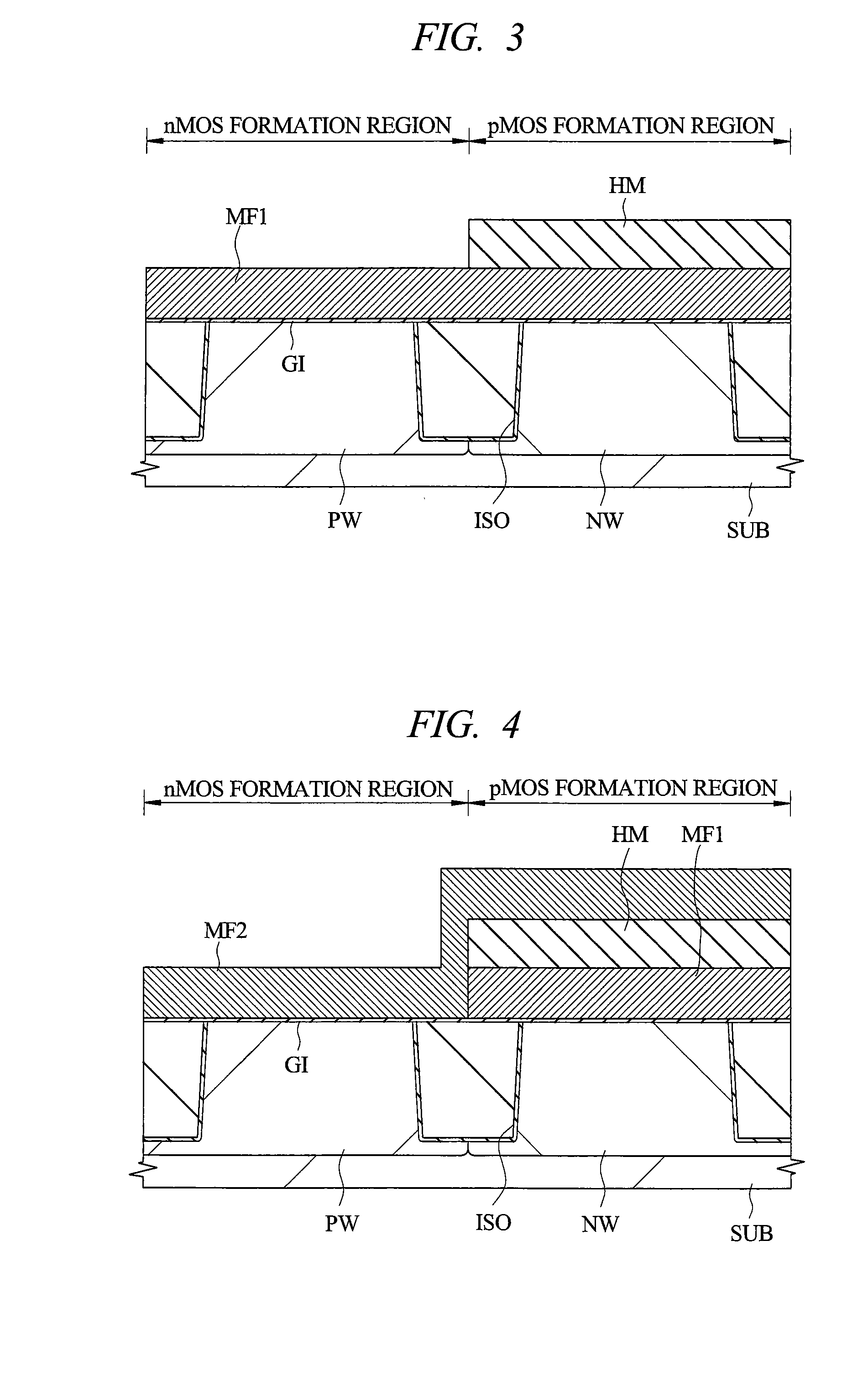
[0087]Although the configuration in which the gate electrode of the n channel MOS transistor is formed of an alloy film containing ruthenium as a base material and hafnium has been described in the first embodiment, the case of a stacked structure in which a hafnium film is deposited on a ruthenium film will be described in the second embodiment.

[0088]The manufacturing method of a CMOS constituted of an n channel MOS transistor and a p channel MOS transistor according to the second embodiment will be described with reference to FIG. 13 to FIG. 15. Note that FIG. 13 is a cross-sectional view showing a principal part of a semiconductor device in the manufacturing process continued from the process described with reference to FIG. 2 in the first embodiment.

[0089]As shown in FIG. 13, the metal film MF1 made of ruthenium is deposited (formed) on the gate insulating film GI made of hafnium-based oxide (hafnium oxide in the second embodiment) by sputtering, and a silicon nitride film is de...

third embodiment

[0101]Although the case where hafnium-based oxide is applied to the gate insulating film of the p channel MOS transistor and the gate insulating film of the n channel MOS transistor has been described in the first and second embodiments, the case where aluminum oxide (Al2O3) is applied thereto will be described in the third embodiment.

[0102]The manufacturing method of a CMOS constituted of an n channel MOS transistor and a p channel MOS transistor according to the third embodiment differs in that aluminum oxide (Al2O3) is used to form the gate insulating film GI in the process described with reference to FIG. 2 after the process described with reference to FIG. 1 in the first embodiment.

[0103]Aluminum oxide is deposited by, for example, the ALD using an O (oxygen) material of H2O and TMA (Trimethylaluminum: AlMe3) of an Al (aluminum) material. Thereafter, PDA is performed thereto in order to reduce the defects in the film.

[0104]This aluminum oxide is the oxide whose relative dielect...


PUM


Abstract

In a p channel MOS transistor and an n channel MOS transistor each having a gate electrode made of metal on a gate insulating film made of oxide whose relative dielectric constant is higher than that of silicon oxide, threshold voltage thereof is reduced. A gate insulating film of a p channel MOS transistor and an n channel MOS transistor is made of hafnium oxide, a gate electrode of the p channel MOS transistor is made of ruthenium, and a gate electrode of the n channel MOS transistor is made of alloy containing ruthenium as a base material and hafnium.

Description

CROSS-REFERENCE TO RELATED APPLICATION[0001]The present application claims priority from Japanese Patent Application No. JP 2007-128691 filed on May 15, 2007, the content of which is hereby incorporated by reference into this application.TECHNICAL FIELD OF THE INVENTION[0002]The present invention relates to a semiconductor device and a manufacturing method thereof. More particularly, it relates to a technology effectively applied to a semiconductor device including a MOS transistor having a gate insulating film made of oxide whose relative dielectric constant is higher than that of silicon oxide (SiO2) and a gate electrode made of metal.BACKGROUND OF THE INVENTION[0003]In a p channel MOS transistor and an n channel MOS transistor constituting a CMOS (Complementary Metal Oxide Semiconductor) circuit, a silicon oxide film is used as a material of a gate insulating film, and a polysilicon film or a stacked film (polycide film) obtained by stacking a metal silicide film such as a tungst...

Claims


Application Information

Patent Timeline
IPC IPC(8): H01L27/092H01L21/28
CPCH01L21/28079H01L21/823842H01L21/82385H01L29/495H01L29/4958H01L29/513H01L29/517H01L29/665H01L29/7833
Inventor NABATAME, TOSHIHIDE
Owner RENESAS TECH CORP
Why Eureka
Try Eureka