MOSFET gate drive with reduced power loss

a technology of mosfet gate drive and power loss, which is applied in the direction of power conversion system, oscillation generator, pulse technique, etc., can solve the problems of reducing the efficiency of the circuit in which the gate drive is employed, affecting the efficiency of the circuit, and affecting the power loss of one megahertz of switching and gate drive, so as to reduce the amount of charge, reduce the power loss of charging and discharging the gate, and improve the overall efficiency of the mos

Inactive Publication Date: 2008-11-27
ADVANCED ANALOGIC TECHNOLOGIES INCORPORATED
View PDF17 Cites 70 Cited by
  • Summary
  • Abstract
  • Description
  • Claims
  • Application Information

AI Technical Summary

Benefits of technology

[0037]These needs are satisfied in a MOSFET that is operated in accordance with this invention, wherein a switching MOSFET is not turned fully off but instead alternates between a fully turned-on condition and a low-current condition. The low-current condition of the MOSFET replaces the fully-off condition that is used in conventional switching sequences. Switching the MOSFET between a fully-on condition and a low-current condition reduces the amount of charge that must be moved to and from the gate of the MOSFET during each switching cycle and thereby reduces the power lost in charging and discharging the gate. In many situations, this power savings more than compensates for the additional power lost from the drain current that continues to flow in the MOSFET in its low-current condition. Therefore the overall efficiency of the MOSFET is improved.

Problems solved by technology

But switching a power MOSFET at frequencies over one megahertz involves switching and gate drive power losses, not just power lost due to conduction.
Conduction and Switching Losses in Power MOSFETs: Even though power MOSFETs offer superior electrical performance to other semiconductor devices, especially for operation below 100 volts, they are not ideal power switches—they do in fact dissipate power and reduce the efficiency of the circuit in which they are employed.
Operating as a controlled current source, the magnitude of a power MOSFET's current must be held to a low value, or the device will overheat.
This phenomenon, known as the Miller effect, greatly complicates calculating power loss with capacitance since during a switching transient, MOSFET 66 passes from cutoff, into saturation, and into its linear region, with the voltage gain and capacitance all varying in tandem.
In such a condition and circuit, the saturated MOSFET exhibits voltage gain, amplifying the gate-to-drain feedback capacitance by constantly changing and increasing amounts, making it increasingly harder for a gate buffer to smoothly drive the MOSFET's gate during the transition.
Instantaneous power losses in the device have peaked and begin to decline as VDS drops.
In the example shown, the current becomes semi-constant during this short interval because the load is inductive and will not allow current to charge instantly.
Since ID, VDS and VGS vary simultaneously, it is difficult to account for all the intra-device currents.
In other words gate drive losses become increasingly critical at higher frequency operation.
In normal applications, where a constant voltage rather than a constant current drive is employed, the gate drive losses are not evident from inspection of the VGS switching waveforms because they occur too quickly to be visible.
The total charge stored on the gate during charging is all lost to ground during turn off.
Such rail-to-rail drive is lossy because it doesn't recycle or preserve any gate charge from cycle-to-cycle and because it drives the gate to a voltage Vcc which may not correspond to the minimum power loss condition shown in FIG. 3B.
As a result, power is wasted by throwing charge away and by overdriving a MOSFETs gate, both factors lowering the efficiency of a converter.

Method used


Image

  • MOSFET gate drive with reduced power loss
  • MOSFET gate drive with reduced power loss
  • MOSFET gate drive with reduced power loss

Examples


Embodiment Construction

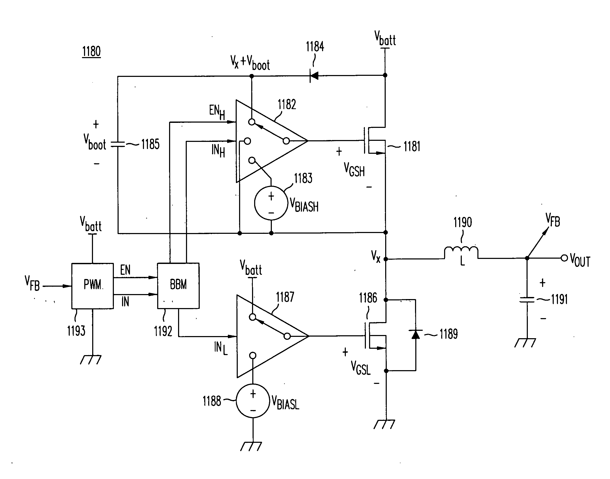
[0104]While power MOSFET design and manufacturing can be used to optimize or minimize the on-resistance gate-charge product of a device used in a power switching application, power losses can also be minimized by limiting the amount of gate charge moved during each switching transition. This task may be achieved in two ways—by limiting the maximum gate drive to an optimum point or by conserving some of the gate charge during switching transitions. This application discloses a means of preserving some gate charge during subsequent switching cycles.

[0105]One embodiment of this invention is illustrated in FIG. 5, where a circuit 200 illustrates a means of driving the gate of a power MOSFET 203 that controls a load 204. Load 204 may comprise any electrical component connected to supply voltage VDD or an electrical network of components connected to both VDD and optionally to ground or to other voltage sources. The input signal to a gate driver 202 is a logic signal output from a buffer ...


PUM


Abstract

A gate driver for a power MOSFET in, for example, a DC-DC converter switches the MOSFET between a fully-on condition and a low-current condition instead of switching the MOSFET between fully-on and fully-off conditions. The amount of charge that must be transferred to charge and discharge the gate of the MOSFET is thereby reduced, and the efficiency of the MOSFET is improved. A feedback circuit may be used to assure that the magnitude of current in the power MOSFET in its low-current condition is correct. Alternatively, a trimming process may be used to correct the magnitude of the voltage supplied by the gate driver to the gate of the power MOSFET in the low-current condition.

Description

CROSS-REFERENCE TO RELATED APPLICATIONS[0001]This application claims the priority of Provisional Application No. 60 / 931,097, filed May 21, 2007, which is incorporated herein by reference in its entirety.FIELD OF THE INVENTION [0002]This invention relates to the driving of discrete or integrated power MOSFETs in switching applications such as DC / DC conversion, and especially switching at high frequencies.BACKGROUND OF THE INVENTION [0003]Switching regulators are used to regulate DC voltages and to convert one DC voltage to another, by stepping the voltage either up or down, or with the ability to step the voltage up or down depending on changing conditions. The quality of a DC / DC switching converter and regulator is measured by its ability to regulate over a range of input voltages, output voltages, load currents and temperatures. It should react sufficiently fast to guarantee good regulation during voltage and current transients as well as during steady state operation. In some appl...

Claims


Application Information

Patent Timeline
Patent Type & Authority Applications(United States)
IPC IPC(8): H03K17/56
CPCH03K17/08142H03K17/145H03K2217/94031H03K17/6872H03K2217/0036H03K17/18H02M1/08H03K17/687
Inventor WILLIAMS, RICHARD K.
Owner ADVANCED ANALOGIC TECHNOLOGIES INCORPORATED
Why Eureka
Try Eureka