Method of fabricating gate oxide layer on silicon carbide material

A gate oxide layer and oxide layer technology, which is applied in semiconductor/solid-state device manufacturing, electrical components, circuits, etc., can solve the problems of the number of trap charges in the interface state and the reduction of oxide layer charges, so as to reduce the number of charges and gate oxidation. Layer densification, quality-enhancing effect

Inactive Publication Date: 2020-02-11
NO 55 INST CHINA ELECTRONIC SCI & TECHNOLOGYGROUP CO LTD
View PDF6 Cites 0 Cited by
  • Summary
  • Abstract
  • Description
  • Claims
  • Application Information

AI Technical Summary

Problems solved by technology

Therefore, this conventional manufacturing method cannot effectively reduce the number of interface state trap charges and oxide layer charges.

Method used


Image

  • Method of fabricating gate oxide layer on silicon carbide material
  • Method of fabricating gate oxide layer on silicon carbide material
  • Method of fabricating gate oxide layer on silicon carbide material

Examples


Embodiment 1

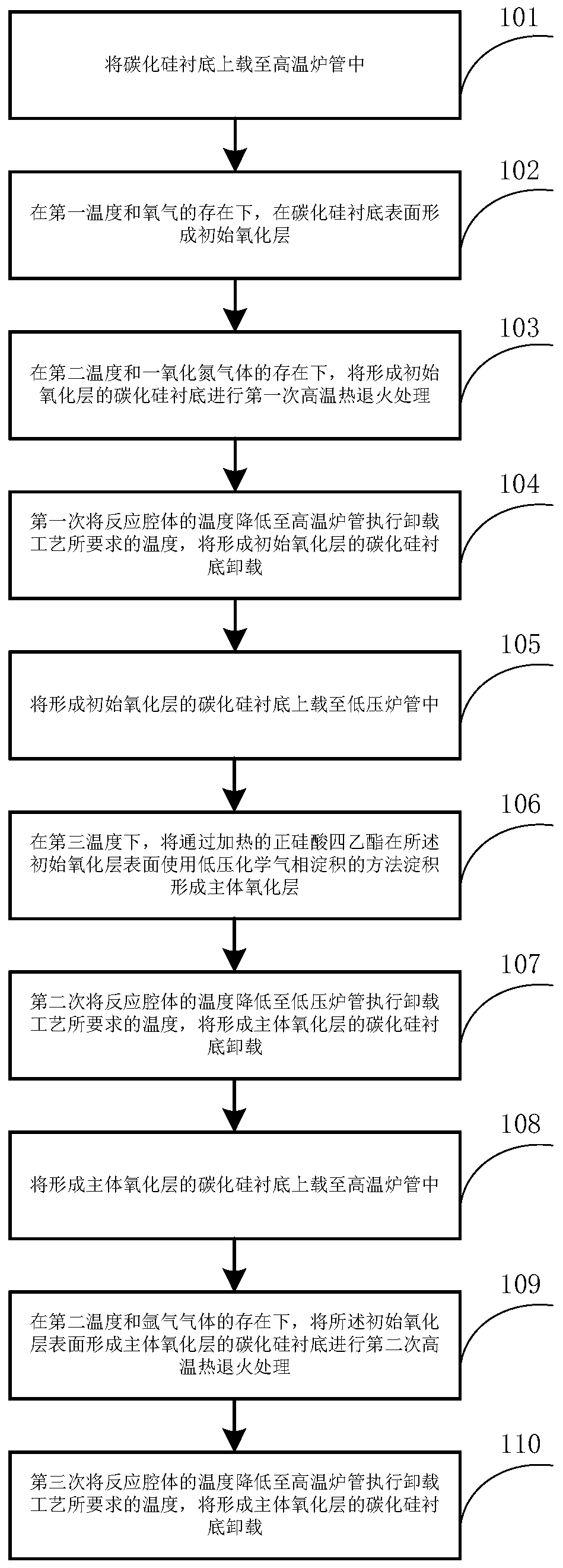
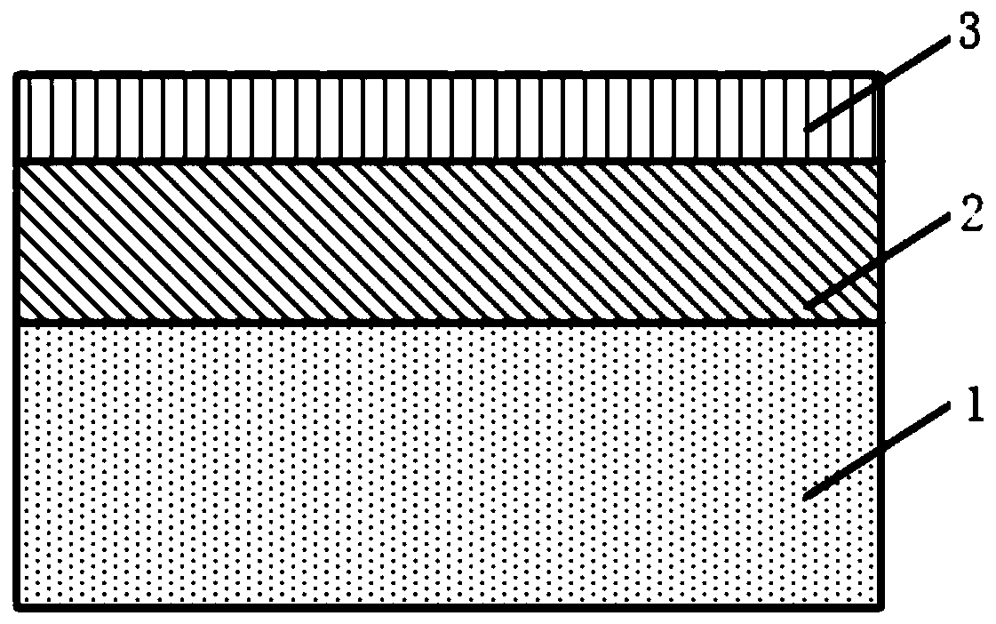
[0050] figure 1 It is a schematic flow chart of the method for manufacturing a gate oxide layer on a silicon carbide material provided in Embodiment 1 of the present invention, image 3 A schematic diagram of the structure obtained by the method for manufacturing the gate oxide layer according to the embodiment of the present invention, as shown in figure 1 and image 3 As shown, the method for manufacturing the gate oxide layer on the silicon carbide material proposed by the present invention comprises the following steps:

[0051] In step 101, a silicon carbide substrate 1 is provided and placed in a high-temperature furnace tube;

[0052] Then set the pressure of the high-temperature furnace tube to 900mbar, and raise the temperature inside the furnace tube to 1150°C at a heating rate of 10°C / min;

[0053] In step 102, oxygen is introduced into the furnace tube, the oxygen flow rate is 1 slm / min, and an initial oxide layer 2 with a thickness of 13 nm is formed on the sur...

Embodiment 2

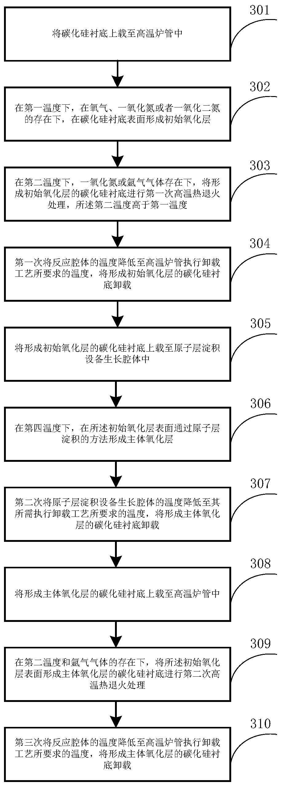
[0066] figure 2 It is a schematic flowchart of a method for manufacturing a gate oxide layer on a silicon carbide material provided in Embodiment 2 and Embodiment 3 of the present invention, image 3 A schematic diagram of the structure obtained by the method for manufacturing the gate oxide layer according to the embodiment of the present invention, as shown in figure 2 and image 3 As shown, the method for manufacturing the gate oxide layer on the silicon carbide material proposed by the present invention comprises the following steps:

[0067] In step 301, a silicon carbide substrate 1 is provided and placed in a high-temperature furnace tube;

[0068] Then set the pressure of the furnace tube to 950mbar, and raise the temperature inside the furnace tube to 1200°C at a heating rate of 10°C / min;

[0069] In step 302, nitrogen monoxide is fed into the furnace tube, the flow rate of nitrogen monoxide is 1 slm / min, and an initial oxide layer 2 with a thickness of 12 nm is ...

Embodiment 3

[0082] figure 2 It is a schematic flowchart of a method for manufacturing a gate oxide layer on a silicon carbide material provided in Embodiment 2 and Embodiment 3 of the present invention, image 3 A schematic diagram of the structure obtained by the method for manufacturing the gate oxide layer according to the embodiment of the present invention, as shown in figure 2 and image 3 As shown, the method for manufacturing the gate oxide layer on the silicon carbide material proposed by the present invention comprises the following steps:

[0083] In step 301, a silicon carbide substrate 1 is provided and placed in a high-temperature furnace tube;

[0084] Then set the pressure of the furnace tube to 1000mbar, and raise the temperature inside the furnace tube to 1000°C at a heating rate of 8°C / min;

[0085] In step 302, nitrous oxide is fed into the furnace tube, the flow rate of nitrous oxide is 0.8 slm / min, and an initial oxide layer 2 with a thickness of 15 nm is formed...


PUM

PropertyMeasurementUnit
thicknessaaaaaaaaaa
thicknessaaaaaaaaaa
thicknessaaaaaaaaaa

Abstract

The invention provides a method of fabricating a gate oxide layer on a silicon carbide material. The method comprises the following steps of: (1) loading a silicon carbide substrate into a high-temperature furnace tube, (2) forming an initial oxide layer on the surface of the silicon carbide substrate at a first temperature in an oxygen atmosphere, (3) carrying out first high-temperature thermal annealing treatment on the silicon carbide substrate at a second temperature in an argon atmosphere, (4) unloading the silicon carbide substrate, (5) loading the silicon carbide substrate to a cavity of a low-pressure furnace tube, and forming a main body oxide layer at a third temperature by using a low-pressure chemical vapor deposition method, (6) unloading the silicon carbide substrate, (7) loading the silicon carbide substrate into the high-temperature furnace tube, (8) carrying out second high-temperature thermal annealing treatment on the silicon carbide substrate at a second temperaturein an argon atmosphere, and (9) unloading the silicon carbide substrate. According to the method, the interface state density and the fixed charge quantity of the oxide layer can be effectively reduced, so that the performance of the gate oxide layer is improved.

Description

technical field [0001] The invention relates to the field of semiconductor device manufacturing, in particular to a method for manufacturing a gate oxide layer on a silicon carbide material. Background technique [0002] With the rapid expansion of the scale of various major economies in human society due to the rapid development of science and technology, a series of global environmental and energy issues have inevitably been introduced. Therefore, environmental protection, high efficiency and energy saving have become key words in the current upgrading of various industries. [0003] Power semiconductor devices and modules have been widely used in electrode regulation, smart grid and power system. To alleviate the global energy crisis, the energy efficiency of such devices must be greatly improved. However, the development of Si devices has approached the theoretical performance limit determined by its material properties. Therefore, new materials must be found to satis...

Claims


Application Information

Patent Timeline
Patent Type & Authority Applications(China)
IPC IPC(8): H01L21/02H01L21/04
CPCH01L21/02164H01L21/02236H01L21/02271H01L21/02293H01L21/02318H01L21/02337H01L21/049
Inventor 费晨曦柏松王谦黄润华陈征张宏伟
Owner NO 55 INST CHINA ELECTRONIC SCI & TECHNOLOGYGROUP CO LTD
Why Eureka
Try Eureka