Resistance memory with tungsten compound and manufacturing

a technology of resistance memory and tungsten compound, which is applied in the field of memory devices, can solve the problems of copper bottom electrode complicating the erasure of memory cells, relative large memory cell size, and large memory cell siz

Active Publication Date: 2008-12-11
MACRONIX INT CO LTD
View PDF1 Cites 134 Cited by
  • Summary
  • Abstract
  • Description
  • Claims
  • Application Information

AI Technical Summary

Benefits of technology

[0003]The present invention relates to memory devices and methods for manufacturing high density memory devices, and more particularly to memory devices having a data storage material based on tungsten-oxygen compounds.

Problems solved by technology

This MIM structure requires several additional masks and patterning to form the noble metal electrodes and the memory material, and results in a relatively large memory cell size.
This structure requires several additional masks to form the top and bottom electrodes, and results in a relatively large memory cell size.
Chen et al. disclose that having a copper bottom electrode complicates erasing of the memory cell since the applied field during erasing may push copper ions into the CuxO.

Method used


Image

  • Resistance memory with tungsten compound and manufacturing
  • Resistance memory with tungsten compound and manufacturing
  • Resistance memory with tungsten compound and manufacturing

Examples


first embodiment

[0099]FIGS. 25-28 illustrate a manufacturing method in accordance with a first embodiment, the manufacturing method resulting in forming the memory device 2400 illustrated in FIG. 24.

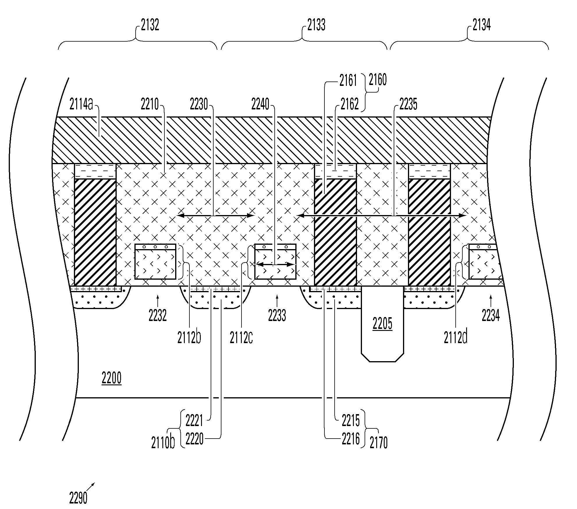
[0100]FIG. 25 illustrates a first step of providing a subassembly including the periphery region 2420 and a memory cell region 2500 on the substrate 2200.

[0101]The memory cell region 2500 includes conductive plugs 2520, 2530, and 2540 each coupled to drain regions of respective access transistors 2232, 2233, and 2234. The plugs 2520, 2530, and 2540 comprise tungsten and extend to the top surface 2460 of dielectric 2210. The top surface 2460 can be formed by example, by a Chemical Mechanical Polishing CMP step after the formation of the plugs 2450, 2520, 2530, 2540 in vias in the dielectric 2210.

[0102]Next, a layer of photoresist 2600 is formed on the periphery region 2420 of the structure illustrated in FIG. 25, resulting in the structure illustrated in FIG. 26. The photoresist 2600 has a thickness 2610...

second embodiment

[0107]FIGS. 29-32 illustrate a manufacturing method in accordance with a

[0108]A dielectric layer 2900 is formed on the top surface 2460 of the dielectric 2210 of the structure illustrated in FIG. 25, and a layer of photoresist 2910 is formed on the portion of the dielectric layer 2900 overlying the logic portion 2420, resulting in the structure illustrated in FIG. 29.

[0109]Next, the dielectric layer 2900 is etched using the photoresist 2910 as a mask, thereby exposing the top surface 2460 of the dielectric 2210 in the memory cell region 2500, resulting in the structure illustrated in FIG. 30.

[0110]Next, an oxygen plasma strip is performed to form the memory portions 2720, 2730, and 2740 from the tungsten material of the plugs 2520, 2530, and 2540 and a wet strip process removes any remaining photoresist 2910, resulting in the structure illustrated in FIG. 31.

[0111]Next, an optional post furnace oxidation step is performed on the structure illustrated in FIG. 31. Because the plug 245...

third embodiment

[0113]FIGS. 33-36 illustrate a manufacturing method in accordance with a

[0114]FIG. 33 illustrates a first step of providing a sub-assembly including the periphery region 2420 and a memory cell region 3300 on the substrate 2200.

[0115]The memory cell region 3300 includes conductive plugs 2520, 2530, and 2540 each coupled to the drain regions of respective access transistors 2232, 2233, and 2234. The memory cell region 3300 also includes a common source line 3310 coupled to the common source region of the access transistors 2232, 2233, the common source line 3310 extending in a direction into and out of the cross-section illustrated in FIG. 33.

[0116]The plugs 2450, 2520, 2530, 2540 and line 3310 comprise tungsten and extend to the top surface 2460 of dielectric 2210. The top surface 2460 can be formed, for example, by a Chemical Mechanical Polishing CMP step after the formation of the plugs 2450, 2520, 2530, 2540 and line 3310 in the dielectric 2210.

[0117]Next, a layer of photoresist i...


PUM


Abstract

Memory devices based on tungsten-oxide memory regions are described, along with methods for manufacturing and methods for programming such devices. The tungsten-oxide memory region can be formed by oxidation of tungsten material using a non-critical mask, or even no mask at all in some embodiments. A memory device described herein includes a bottom electrode and a memory element on the bottom electrode. The memory element comprises at least one tungsten-oxygen compound and is programmable to at least two resistance states. A top electrode comprising a barrier material is on the memory element, the barrier material preventing movement of metal-ions from the top electrode into the memory element.

Description

CROSS-REFERENCE TO RELATED APPLICATIONS[0001]This application claims the benefit of U.S. provisional patent application No. 60 / 943,300 entitled “Methods of Manufacturing Embedded Resistance Memory with Tungsten Compound” filed on 11 Jun. 2007, which is incorporated by reference herein.BACKGROUND OF THE INVENTION[0002]1. Field of the Invention[0003]The present invention relates to memory devices and methods for manufacturing high density memory devices, and more particularly to memory devices having a data storage material based on tungsten-oxygen compounds.[0004]2. Description of Related Art[0005]Nonvolatile memory devices include magnetic random access memory MRAM, ferroelectric random access memory FRAM and phase-change random access memory PCRAM and other resistive random access memory RRAM. RRAM has attracted much attention because of its simple structure and small cell size.[0006]Metal-oxide based RRAM can be caused to change resistance between two or more stable ranges by appl...

Claims


Application Information

Patent Timeline
Patent Type & Authority Applications(United States)
IPC IPC(8): G11C11/00H05H1/24
CPCB82Y10/00G11C11/14G11C11/22G11C11/5685G11C13/0007G11C2213/32G11C2213/51G11C2213/79H01L27/2436H01L45/04H01L45/1233H01L45/146H01L45/1633H01L45/1683H10B63/30H10N70/20H10N70/028H10N70/8833H10N70/826H10N70/066
Inventor HO, CHIAHUALAI, ERH-KUN
Owner MACRONIX INT CO LTD
Why Eureka
Try Eureka