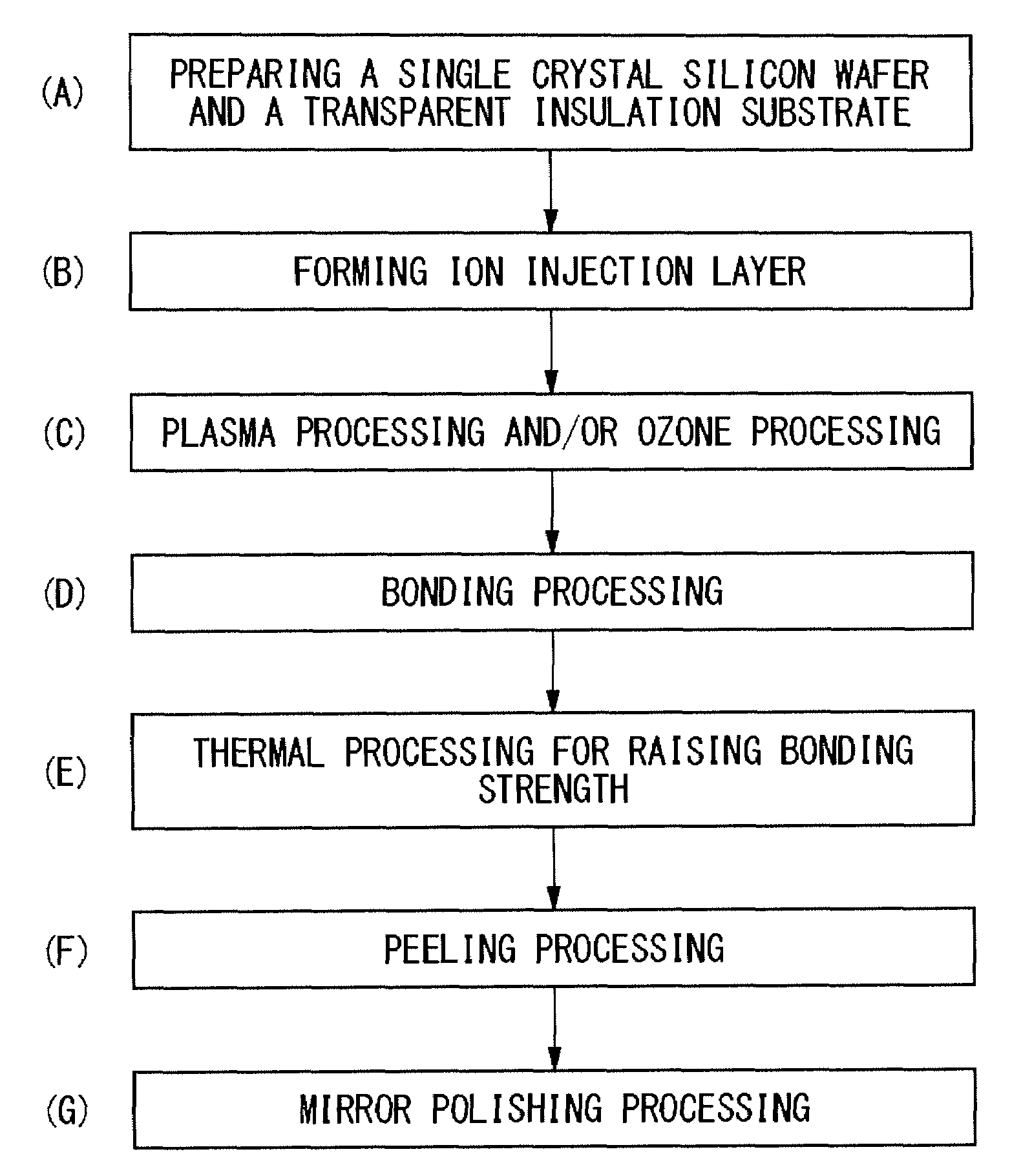
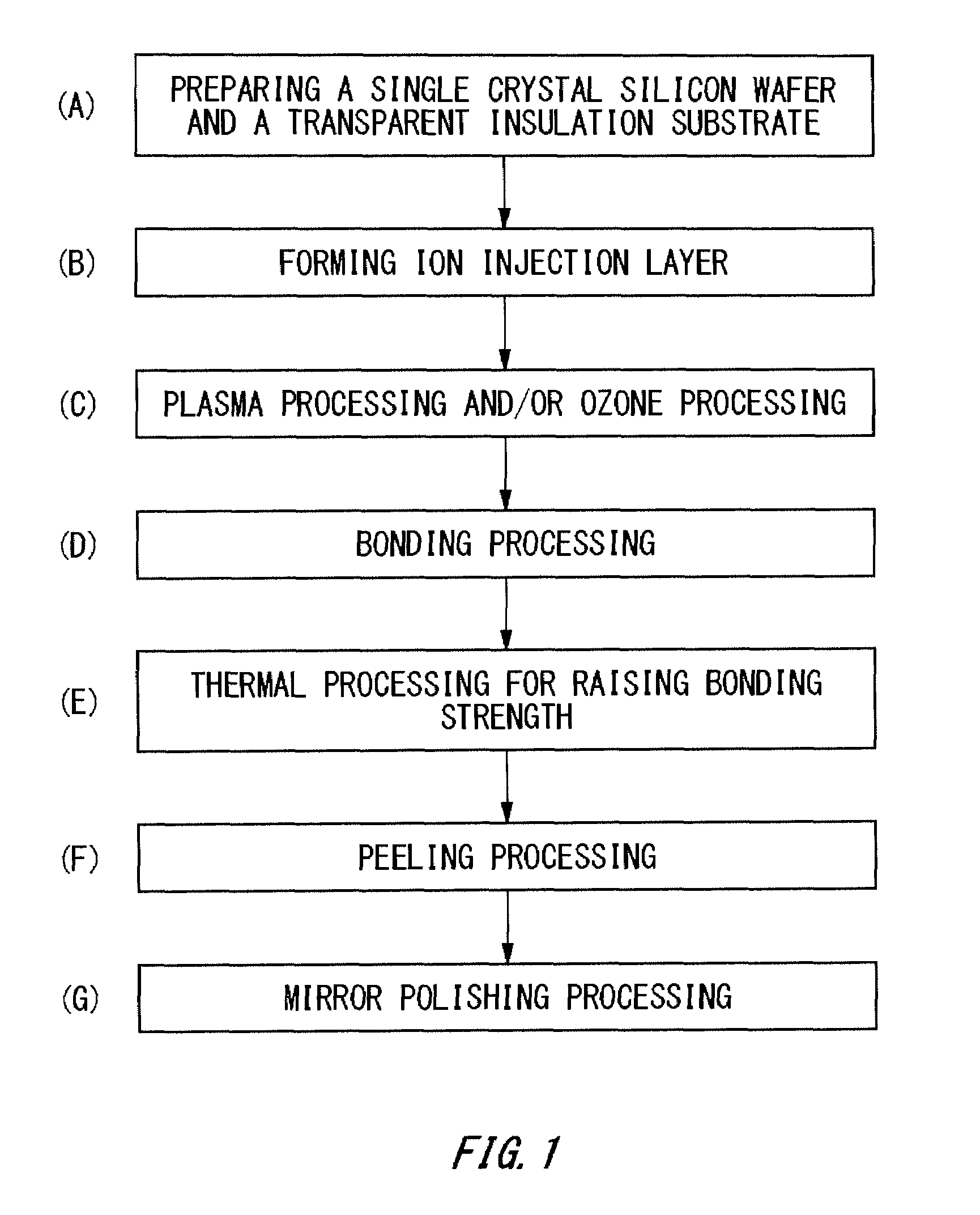
Silicon on insulator (SOI) wafer and process for producing same
a technology of silicon on insulator and soi, which is applied in the direction of layered products, chemistry apparatus and processes, and synthetic resin layered products, etc., can solve the problems of cracking or breaking of silicon substrate or soi layer, and achieve good film thickness uniformity, excellent crystallization, and thin film thickness
- Summary
- Abstract
- Description
- Claims
- Application Information
AI Technical Summary
Benefits of technology
Problems solved by technology
Method used
Image

Examples
embodiment example
[0049]A single crystal silicon wafer having a diameter of 200 mm and one surface thereof being subjected to mirror polishing is prepared, as a wafer for forming an SOI layer. A silicon oxide layer of 100 nm is formed on the surface of the single crystal silicon wafer by thermal oxidization. The surface roughness (Ra) of the oxide layer at the surface subjected to mirror polishing (i.e. a surface to be bonded) was 0.2 nm. The measurement was performed to the measurement region of 10 μm×10 μm using an atom force microscope.
[0050]As a transparent insulation substrate, a synthetic silica wafer having a diameter of 200 mm and one surface thereof being subjected to mirror polishing is prepared. The surface roughness (Ra) of the transparent insulation substrate at the surface subjected to mirror polishing (i.e. a surface to be bonded) was 0.19 nm. The apparatus and the method of measuring have the same condition as the oxide layer of the single crystal silicon wafer.
[0051]A hydrogen ion is...
PUM
| Property | Measurement | Unit |
|---|---|---|
| temperature | aaaaa | aaaaa |
| thickness | aaaaa | aaaaa |
| temperature | aaaaa | aaaaa |
Abstract
Description
Claims
Application Information