High Temperature Processing Compatible Metal Gate Electrode For pFETS and Methods For Fabrication

a technology of metal gate electrode and high temperature processing, which is applied in the direction of transistors, electrical devices, semiconductor devices, etc., can solve the problems of halogen incorporation, high growth temperature, and damage to the gate dielectric field, and achieve the effect of reducing the number of halogen incorporation and high growth temperatur

Inactive Publication Date: 2008-12-18
GLOBALFOUNDRIES INC
View PDF24 Cites 3 Cited by
  • Summary
  • Abstract
  • Description
  • Claims
  • Application Information

AI Technical Summary

Benefits of technology

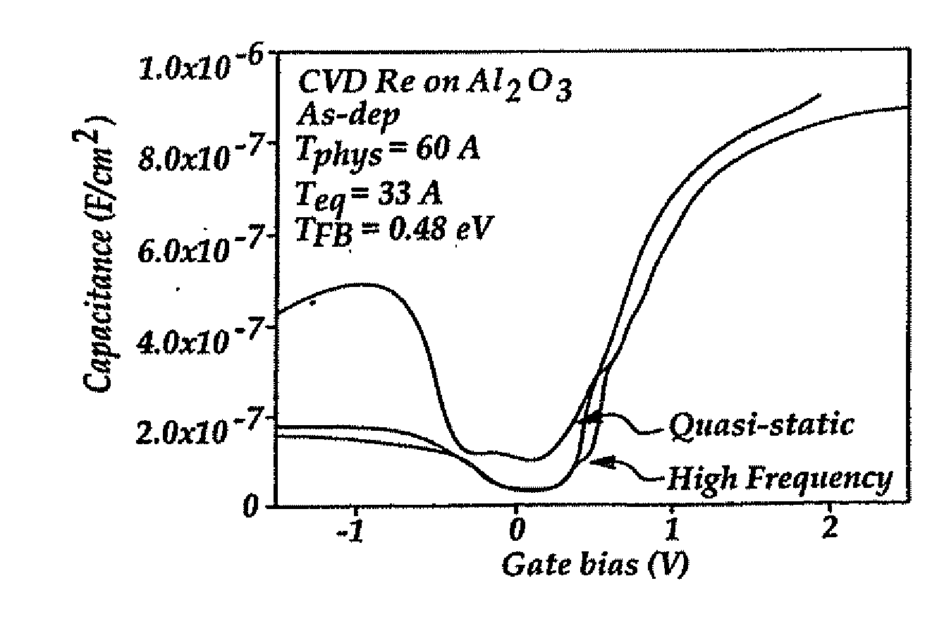
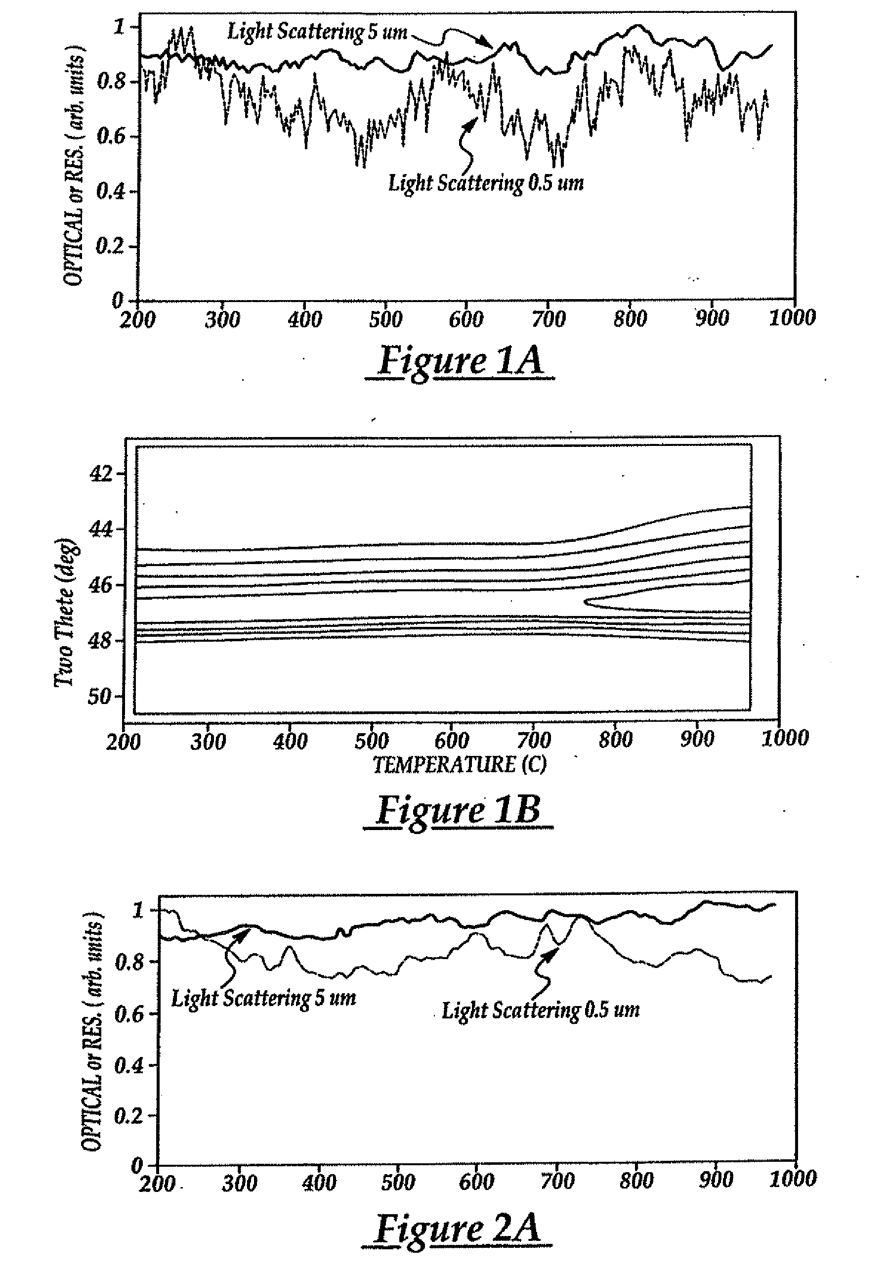
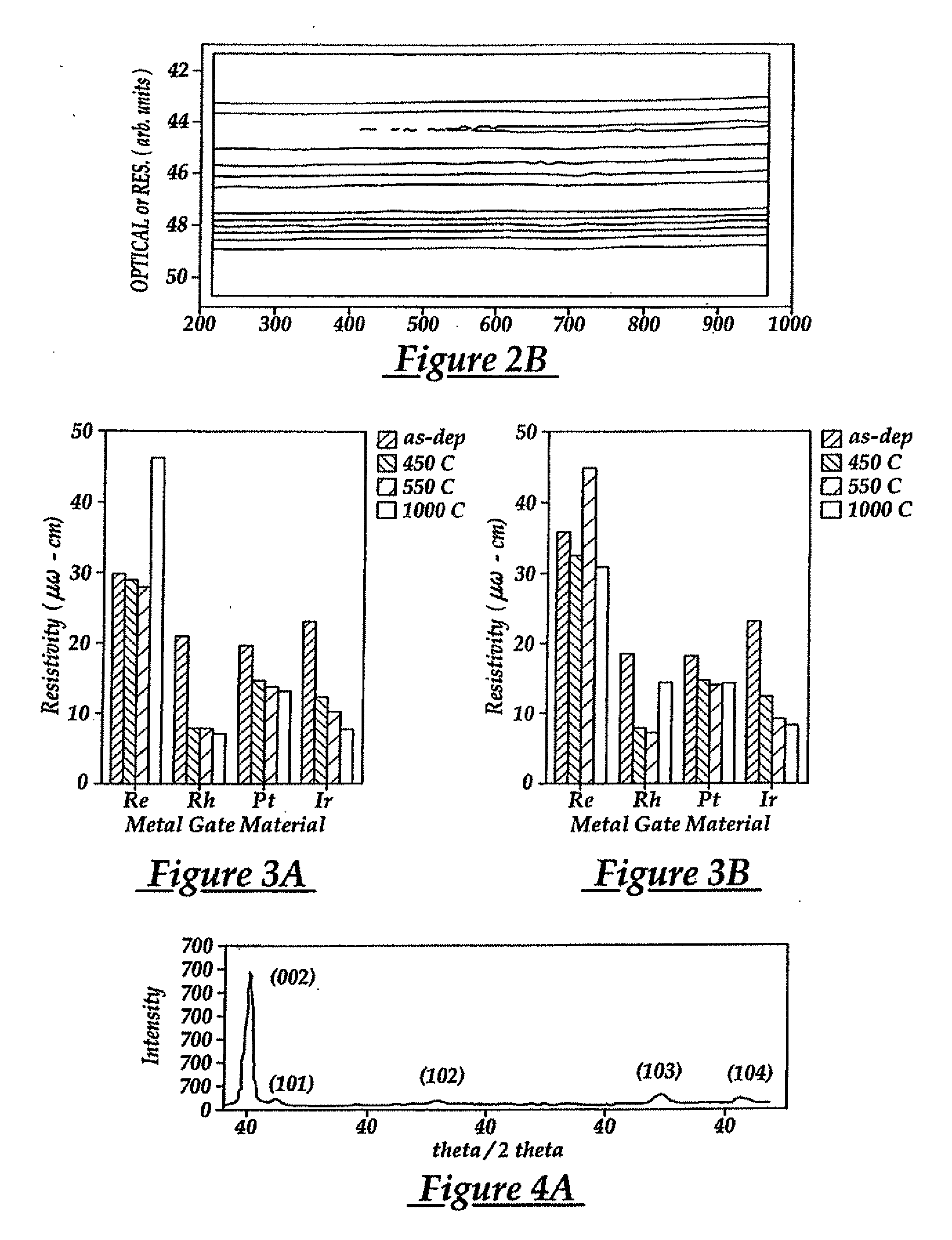
[0011]The invention provides a method for fabricating a CMOS gate electrode by using a Re, Rh, Pt, Ir or Ru metal. The work functions of these metals make them compatible with current pFET requirements. For instance, when Re is used, it can withstand the high hydrogen pressures necessary to produce properly passivated interfaces without undergoing chemical changes. Its thermal stability on SiO2, Al2O3, ZrO2, HfO2 and a variety of other dielectrics makes it compatible with post processing temperatures up to 1000° C. The present invention method allows the fabrication of FETs and to passivate the metal / dielectric interfaces of these FETs to better than Dit=5E10 / cm2 eV interface states.
[0012]The pFET metal gate avoids the problem of poly-Si depletion and allows for a reduction in the effective capacitance of the device gate stack. The use of a metal gate allows for a thicker gate dielectric than would otherwise be required with a poly-Si gate. At the same time, the thermal stability of these metal gate materials make them fully compatible with standard post-processing techniques, i.e. activation anneals and the like.

Problems solved by technology

Other physical vapor deposition processes such as sputtering and e-beam evaporation lead to gate dielectric damage which is thought to be a long-term reliability problem even if some damage may be repaired by a forming gas or by a hydrogen anneal treatment.
While the deposition of Re metal by using a chemical vapor deposition technique has been attempted by others in the art, the deposited Re films using a halide precursor causes problems of halogen incorporation and high growth temperatures.

Method used


Image

  • High Temperature Processing Compatible Metal Gate Electrode For pFETS and Methods For Fabrication
  • High Temperature Processing Compatible Metal Gate Electrode For pFETS and Methods For Fabrication
  • High Temperature Processing Compatible Metal Gate Electrode For pFETS and Methods For Fabrication

Examples


Embodiment Construction

[0034]The present invention discloses a method for fabricating a CMOS gate electrode incorporating Re, Rh, Pt, Ir or Ru metal. The work functions of these metals make them compatible with current p-FET requirements. The requirements of the p-FET gate material, presented below, are divided into four sections of deposition techniques, physical characterization, electrical characterization and integration.

Deposition Techniques

[0035]The Re electrode fabrication in the present invention is achieved by using a low temperature / low pressure CVD technique with Re2(CO)10 as the source material. Specifically, the method of the present invention comprises the steps of (a) depositing a uniform layer of Re directly onto a dielectric material such as an ultra-thin gate dielectric material, the dielectric material being positioned on a semiconductor substrate, the deposition is carried out by CVD using Re2(CO)10 as the source material under conditions which are sufficient to form the Re layer; and ...


PUM

PropertyMeasurementUnit
temperatureaaaaaaaaaa
temperaturesaaaaaaaaaa
total pressureaaaaaaaaaa

Abstract

A method for fabricating a CMOS gate electrode by using Re, Rh, Pt, Ir or Ru metal and a CMOS structure that contains such gate electrodes are described. The work functions of these metals make them compatible with current pFET requirements. For instance, the metal can withstand the high hydrogen pressures necessary to produce properly passivated interfaces without undergoing chemical changes. The thermal stability of the metal on dielectric layers such as SiO2, Al2O3 and other suitable dielectric materials makes it compatible with post-processing temperatures up to 1000° C. A low temperature / low pressure CVD technique with Re2(CO)10 as the source material is used when Re is to be deposited.

Description

RELATED APPLICATION[0001]This application is a division of U.S. application Ser. No. 09 / 995,031, filed Nov. 29, 2001.FIELD OF THE INVENTION[0002]The present invention generally relates to a metal gate electrode for p-type field effect transistors and a method for fabricating the electrode and more particularly, relates to a metal gate electrode that is compatible with high temperature processing of p-type FETs and a method for fabricating the electrode.BACKGROUND OF THE INVENTION[0003]In the fabrication of complimentary metal oxide semiconductor (CMOS) integrated circuit devices with metal gates, deposition methods for the gate metals which include thermal evaporation (from Knudsen cells) and chemical vapor deposition are preferable since they lead to minimal gate dielectric damage and minimal long-term reliability problems. Other physical vapor deposition processes such as sputtering and e-beam evaporation lead to gate dielectric damage which is thought to be a long-term reliabilit...

Claims


Application Information

Patent Timeline
Patent Type & Authority Applications(United States)
IPC IPC(8): H01L21/44H01L21/28H01L21/285H01L21/30H01L21/336H01L29/423H01L29/49H01L29/78H01L29/786
CPCH01L21/28079H01L29/495H01L21/3003H01L21/18
Inventor AMOS, RICKYBUCHANAN, DOUGLAS A.CABRAL, JR., CYRILCALLEGARI, ALESSANDRO C.GUHA, SUPRATIKKIM, HYUNGJUNMCFEELY, FENTON R.NARAYANAN, VIJAYRODBELL, KENNETH P.YURKAS, JOHN J.
Owner GLOBALFOUNDRIES INC
Why Eureka
Try Eureka