

Method of forming metal pattern, patterned metal structure, and thin film transistor-liquid crystal displays using the same
a thin film transistor and liquid crystal display technology, applied in metallic pattern materials, resistive material coatings, solid-state devices, etc., can solve the problems of increasing resistance of lines in metal patterns, deteriorating display quality of electronic devices, and becoming an obstacle to the development of tft-lcds with high image quality and large area, so as to reduce costs, simplify processes, and manufacture larger tft-lcd displays
- Summary
- Abstract
- Description
- Claims
- Application Information
AI Technical Summary
Benefits of technology
Problems solved by technology
Method used
Image

Examples
example 1
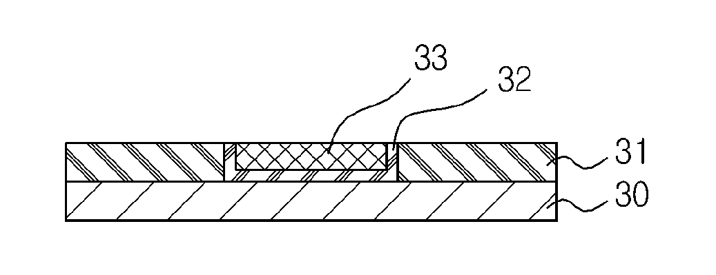
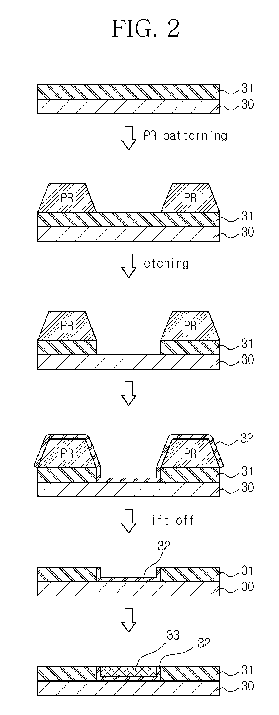
[0068]A silicon nitride dielectric substrate was formed by depositing a silicon nitride film having a thickness of 400 nanometers (nm) on an insulated glass substrate using chemical vapor deposition. Subsequently, a photoresist (AZ-1512, manufactured by Clariant International Ltd.) was applied on the silicon nitride dielectric substrate using a spin-coating method at a rotation speed of 1200 rpm, at room temperature, for 30 seconds, and at a viscosity of 20 centipoise. Then, the substrate coated with the photoresist was patterned by exposing the applied photoresist for 7 seconds using ultraviolet-exposure (broad band UV with power of 9 milli Joules per square centimeter), available from Oriel Inc., as a light source through a photomask, and then developing the exposed photoresist. The exposed portion of the photoresist was removed from the patterned substrate using a hydrogen fluoride solution having a concentration of 0.25 weight percent (wt %) for 200 seconds.
[0069]Subsequently, a...
PUM
| Property | Measurement | Unit |
|---|---|---|
| Temperature | aaaaa | aaaaa |
| Dielectric polarization enthalpy | aaaaa | aaaaa |
| Electrical conductor | aaaaa | aaaaa |
Abstract
Description
Claims
Application Information